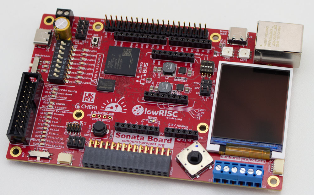
Sonata system
Sonata is a system for evaluating the usage of the CHERIoT Ibex core as a microcontroller for embedded, IoT and Operational Technology applications. The system contains a number of peripherals (I2C, SPI, GPIO, USB, and UART) and the CHERIoT Ibex core itself. It is designed for use on FPGA and specifically targets the Sonata FPGA board, but as the entire design is open-source (from PCB to software), it can be run on any similar system.
This project is designed to look like a normal microcontroller in terms of usability, including SDK, examples, and normal capabilities such as debuggers. But underneath that the CHERIoT capabilities provides a high level of "default security" that simplifies designing embedded systems in a secure manner. You can see the complete documentation for the project. Sonata is part of the Sunburst Project funded by UKRI / DSbD under grant number 107540.

Current status
We are delighted to announce the release of the Sonata system! The latest release is available on GitHub here.
This new release provides a base FPGA image with I2C/SPI/UART peripherals that are suitable for use with the expansion headers as well as the on-board hardware.
On the software side a full build flow for Microsoft's CHERIoT RTOS is available along with driver support for the Sonata peripherals in the sonata-software repository. A flash bootloader enables easy 'drag and drop' programming where a generated UF2 is copied to Sonata’s virtual USB drive (in a similar manner to the RP2040 and arm Mbed platforms). Environment setup and build instructions are available for Windows, macOS and Linux.
If you find any issues with the Sonata system, or have features you would like to propose, please create an issue on GitHub. For support with the board itself please use the forum on the NewAE website, create an issue on the sonata-pcb repository, or reach out to NewAE directly.
Getting started
If you have a Sonata board, you can jump to the Getting Started guide. This will walk you through plugging in the board, building example software, and programming the software. For more advanced usage, you can see a Reference Manual similar to what a normal microcontroller reference manual (peripherals, features, etc.) and then see the FPGA development flow if you wish to modify the soft-core itself.
You can also work with a simulated environment, and there is a nice guide on this in the sonata-software documentation. This simulates the entire in Verilator, allow you to develop both hardware (the FPGA) and software (running code) programs.
Documentation introduction
This documentation is built using mdBook. If you are reading this file in GitHub, you should instead see the pre-built documentation on the lowRISC Website which includes the full documentation.
If you'd like to build a copy of the documentation locally, see the Building Documentation page.
License
Unless otherwise noted, everything in the repository is covered by the Apache License, Version 2.0. See the LICENSE file for more information on licensing.
Getting started with the Sonata board
This guide helps you to get started with the Sonata board by building code with CHERIoT technology enabled. One more advanced feature of Sonata is you can adjust the number and type of peripherals included. This is described in the section FPGA Development, for this getting started guide you will use one of the default setups.
The Sonata board is a prototype board and is under active development. This documentation is in the process of being updated. Some parts of the documentation may be out of date or otherwise confusing because of this. This getting started material and the documentation in the sonata-software repository provides the best material for new users to focus on.
See the following section for steps getting started steps on how to update the Sonata system.
Updating the Sonata System
To get started with your Sonata board, there are three levels of hardware/software designs you'll need to be able to load onto the board.
First, head to the Sonata System Release Page where you'll find the latest releases. Each release includes an RP2040 firmware image and FPGA bitstream. Once you have downloaded these, proceed with the following tasks:
- Program the RP2040 With the latest firmware to get any bug fixes by entering bootloader mode & dragging the
rpi_rp2_vX.Y.uf2. - Get the latest FPGA image that corresponds with the software you are building. This requires you to just drag the new
sonata-vX.Y.bit.slot1.uf2file into the 'SONATA' drive that comes up when you plug in the board to your computer. - Build the example code and download to the soft-core you loaded in step 1.
Follow along each of the following sections to complete these tasks.
Reloading the RP2040 USB Controller
Before plugging in your Sonata board, hold down the SW9 labelled "RP2040 Boot", and while holding this button plug your board into your laptop using the Main USB.
A drive called 'RPI-RP2' should pop up on your computer and drag rpi_rp2_vX.Y.uf2 into it.
This drive should automatically dismount once the file is transferred and remount as 'SONATA'.
Downloading the rpi_rp2_vX.Y.uf2 file
Currently the RP2040 firmware is available from the Sonata Systems release page, which ensures your RP2040 firmware matches the Sonata FPGA and firmware expectations.
The source & latest release for the RP2040 are also found on the Sonata RP2040 repo.
Reloading the FPGA Image
The first thing you should do before building the firmware is to get the latest version of the FPGA image, called the "bitstream". This contains the configuration for the microcontroller core & peripherals. The "release version" of the bitstream must match the configuration you use to build the software, as if the bitstream is a different version than what the software is expecting, you are not going to have fun!
When you download a release from the Sonata System page, you'll have a matching bitstream and software setup.
While you can build your own bitstream as described in FPGA Development, we recommend starting with our prebuilt bitstream first. Building the bitstream requires installing Vivado which takes a large amount of hard drive space and requires a separate manual installation process (as well as the build process is much slower than a software compile, so adds delay until you can play with CHERIoT).
Selecting a Bitstream
When the Sonata board is plugged in, it loads one of three bitstreams. This is selected by the switch below the USB port labeled "Bitstream":
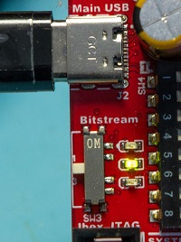
The LEDs besides the switch show the current image selected as well for confirmation.
The slot used by a bitstream is selected by the UF2 file. The bitstream UF2s provided in the release are labeled with which slot they use in the filename.
Drag & Drop Programming
To program the Sonata bitstream:
- Download the bitstream from our releases.
- Make sure that you have the bitstream switch (SW3) set to 1.
- Plug in your Sonata board using the main USB. You should see a 'SONATA' drive (see troubleshooting section if unsure).
- Copy the updated FPGA
sonata-vX.Y.bit.slot1.uf2file to the drive and wait for the copy to complete (on Linux note the copy command may return immediately, so you need to wait until it's done.) - The board should automatically restart once the image is copied over. You should see the 'FPGA Config' LED come on:
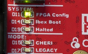
This indicates the FPGA configuration succeeded. This LED should stay on. You should also see the Ibex Boot LED come on indicating the processor core has booted.
The
FPGA ConfigLED reflects the state of the FPGADONEpin. If this LED is not on your board will not work, as there is no logic (core) loaded, or it has become corrupted. This is true even if you are not building Sonata designs but using the board as a general-purpose FPGA board. See troubleshooting below if this LED does not come on, or appears to only come on briefly.
Programming on Power Cycle
Once the copy completes (it can take from 15-120 seconds), you should see the device reboot and the Ibex boot LED come on as mentioned. If you unplug & re-plug the USB cable, it will also reprogram the FPGA. The bitstream is stored on FLASH memory on the Sonata board.
Troubleshooting
Sonata Mass Storage Drive Issues
The Sonata board when plugged in should show a mass storage drive with these files:
LOG.TXT
OPTIONS.TXT
README.TXT
If the board has a RPI loader, visible because you'll see the file INFO_UF2.txt with the contents Model: Raspberry Pi RP2, you may need to reload the RP2040 as described in the Sonata Board Updating Firmware section. This could
be because the RPI Boot button was held down when plugging in the board.
The Sonata board will print status and messages to the LOG.TXT which can be helpful for debugging. It should show the status of valid-looking bitstreams:
TEST CRC Test PASS
CRIT: FW_VER 0.4.0
INFO: Bitstream found in slot 0
INFO: Bitstream found in slot 1
INFO: Bitstream found in slot 2
INFO: Firmware found in slot 0
INFO: No firmware in slot 1
INFO: No firmware in slot 2
INFO: Using slot 0
INFO: Bitstream in flash @ 0, programming 18AC70 bytes...
INFO: Finished programming CRC=98E5AFD6
INFO: Bitstream prog success
FPGA Config LED not coming on
If the FPGA Config LED is not coming on, this could indicate the bitstream was designed for a different FPGA, or some other hardware issue. This should be troubleshooted with the OpenFPGALoader utility as described further down this page.
Ibex Boot LED not coming on
If the FPGA Config LED is on but the Ibex Boot LED is not, it may be that you have programmed (or selected) a different bitstream than one that runs the CHERIoT demo. Try reloading the bitstream, and try power cycling the device.
Device Rebooting During/After Programming (No Serial Activity)
The Sonata board takes a fair amount of power (>500mA) from the USB interface, and should be connected via USB-C. Typically it is close enough to the USB 2.0 limits that it will work with the adapter most of the time, but if you are having reliability issues we recommend trying a different computer, ideally one with a USB-C port.
If you use a recent openFPGALoader build from at least May 25, 2024 you can print the min/max VCCINT ranges. To do this, simply run:
openFPGALoader -c ft4232 -X
This will print several XADC values, pay careful attention to minvccint:
{"temp": 39.9061,
    "maxtemp": 40.3194,
    "mintemp": 25.9852,
"raw":  {"0": 40684, "1": 21949, "2": 39270, "3": 0, "4": 0, "5": 0, "6": 21948, "7": 0},
"vccint": 1.00415,
   "maxvccint": 1.00635,
   "minvccint": 1.00195,
"vccaux": 1.79663,
   "maxvccaux": 1.79883,
   "minvccaux": 1.79517,
}
The minvccint and maxvccint should be fairly close as shown here. Larger ranges indicate possible ringing, or a minvccint near or below 0.95V indicates a brown-out. You can compare the results of loading a different bitstream to see what is normal for your board.
See note below about if you get permissions error running openFPGALoader.
FPGA Programming via USB/JTAG
If for some reason the mass storage programming isn't working, you can also use the built-in FTDI JTAG programming. This requires the setup described in FPGA Programming to build openFPGALoader. Once built, you simply run:
openFPGALoader -c ft4232 sonata_top.bit
Note this requires the udev setup described in FPGA Programming. If you are lazy you can just run the command as root instead (not recommended, but can be helpful for troubleshooting on VMs):
sudo openFPGALoader -c ft4232 sonata_top.bit
You can also check if the flag --read-register STAT is available (newer than 0.12.2 is needed) which will print detailed information about the configuration status with a recent version of openFPGALoader. This is especially helpful if you are trying to understand why the DONE LED is not coming on:
CRC Error      No CRC error
Part Secured   0
MMCM lock      1
DCI match      1
EOS            0
GTS CFG B      0
GWE            0
GHIGH B        0
MODE           7
INIT Complete  1
INIT B         0
Release Done   0
Done           0
ID Error       ID error
DEC Error      0
XADC Over temp 0
STARTUP State  0
Reserved       0
BUS Width      x1
Reserved       8
Building Examples
The following contains some simple examples you can build for the Sonata board. These include CHERIoT-RTOS-based examples from the Sonata software repository, and baremetal examples for advanced-users from this repository. Once you've got one or both of these builds working, you can easily add more features to the example code.
Using our template
Please go to the Sonata software repository using the branch appropriate to your release and build a full application from there. Inside your setup you should simply be able to build it like this:
git clone --recurse-submodule \
    https://github.com/lowRISC/sonata-software.git
cd sonata-software
nix develop .
xmake -P examples/
After running this you should see the build run to completion and report success, the critical lines indicating a successful build are (note output size may differ):
Converted to uf2, output size: 74752, start address: 0x101000
Wrote 74752 bytes to build/cheriot/cheriot/release/sonata_simple_demo.uf2
[100%]: build ok, spent 6.827s
You can drag and drop this UF2 file into the SONATA drive to program the firmware.
UART output
On Linux use the following command to check you can receive serial output:
screen /dev/ttyUSB2 921600
On Mac this is similar
screen /dev/tty.usbserial-LN100302 921600
On Windows, connecting to serial ports directly from within WSL2 (default) is not possible. Connecting from WSL1 is possible, but we recommend to use PuTTY to connect to serial ports. Alternatively you can use Termite.
Select "Serial" as "Connection type", put the COM port in the "Serial line" text field, and set "Speed" to 921600. To find out what serial ports are available, you can open Device Manager and all connected serial ports are listed under "Ports (COM & LPT)" section.
Baremetal examples
This is only for advanced users. If you want to build the baremetal examples in the Sonata repo you can follow these instructions.
First setup a toolchain. Note none of the current Nix environments have exactly the correct set of dependencies to build the baremetal examples. This will change but for the time being you either need to alter a Nix environment (either add cmake to the sonata-software environment or the CHERIoT toolchain to the sonata-system environment) or setup a toolchain outside Nix.
Additional Toolchain Setup
Besides the compiler, there are a few more features the example code depends on.
SRecord Tools
The build environment uses srecord tools, which you can install with:
sudo apt install srecord
CHERIoT LLVM
IMPORTANT: Set this environmental variable to the llvm build you did in the previous part:
export CHERIOT_LLVM_BIN=/path/to/cheriot-llvm/bin
WARNING: The path to
/path/to/cheriot-llvm/binshould point to the build directory you created, not just the root checked outcheriot-llvmdirectory. The path will look something like:~/llvm-tools/cheriot-llvm/builds/cheriot-llvm/bin
Please make sure you unset the CHERIOT_RTOS_SDK environment variable as cmake will automatically pull in the correct version.
The following assumes you have run the source .venv/bin/activate command in the terminal you are using, and you are currently at the root directory of your local sonata-system git repository.
Building Baremetal Examples
To build, run the following from the root of the directory which will build the examples:
cmake -B sw/cheri/build -S sw/cheri
cmake --build sw/cheri/build
The build output is put in the sw/cheri/build directory.
Two files of interest are created for each target: an ELF file which has no extension and a *.vmem file.
The *.vmem file can be used to load directly into the FPGA bitstream, described in more detail on the Programming the Sonata Software page.
If you get an error that
CMake will not be able to correctly generate this project., check back in the list to see if you see an error within the output similar toclang: error: unknown argument: '-mxcheri-rvc'. If this happens it means the wrong (non-CHERIoT) compiler was used. Check back to see what compiler is being used.
Loading software onto the FPGA
You can load software onto the FPGA over USB (JTAG) using:
./util/mem_helper.sh load_program -e sw/cheri/build/tests/spi_test
There are actually four different ways of loading the program - we normally use JTAG for development, but you can also program it into the serial flash device on the board. See the page Programming the Sonata Software.
Developer Guide
The Sonata architecture comprises a number of components:
- Physical board architecture: This is the board that hosts the FPGA (field programmable gate array), all other components, headers and interfaces.
- FPGA configuration architecture: It defines everything we are using a hardware description language for. This includes hardware IP blocks and bus architecture.
- Software architecture: This includes toolchain, operating system and applications.
Before we go into the architecture of the system, it is good to understand the use cases that we are envisioning, so that we can derive our architectural requirements from that.
Use cases and requirements
The Sonata is meant to be used by academics and industry users who are interested in experimenting with CHERIoT in embedded and IoT applications. This is the main reason why we are building a custom FPGA board so that we can make the platform easily usable. We also need the board to be as affordable as possible while still being performant and usable.
This ease of use comes in handy for classroom and demonstration use cases, for which we think this board will come in quite handy. In the classroom, it is also pertinent that we have a debuggable system.
Because we are focussing on embedded and IoT applications, we need to ensure connectivity. This includes being connectable to standard peripherals as well as being extendable with functionality required for niche use-cases.
The other major benefit of creating a custom board is that we can highlight CHERIoT specific features. We envision users of this board to want to show off and experiment with the new CHERIoT technology. If they are using the board as a demonstrator they will want to show off the prowess of CHERI, and if they are experimenting with the board they will want CHERI to be visible.
Like most physical boards, it is nice for it to be as interactive as possible. This means being able to accept user input and respond to them visibly and in an interactive way.
Beyond the physical Sonata board, we expect the soft design that is used to configure the FPGA to also be integrable into a bigger design. For example, we envision it being connected to OpenTitan Earl Grey through a bridge interface.
In short, these are our general requirements:
- Usable
- Affordable
- Debuggable
- Connectable
- Extendable
- CHERI visible
- Interactive
- Integrable
Detailed specifications
Toolchain
The toolchain will build on top of the work already done on CHERIoT, which uses a fork of LLVM. Through Sonata, we are not proposing any changes to the CHERIoT instruction set. We may need some changes to allow code to be stored in memory that does not have associated tags.
The toolchain for software development is described in the Software toolchain setup section. If these instructions ever go out of date, you should be able to find the up to date instructions to build the toolchain from the CI YAML file.
Applications
Especially for the usable and CHERI-visible requirements, it is important that we have a set of demonstration applications. One demonstration application is cycling through each of the CHERIoT exception types with code snippets showing what went wrong. We can show what happens when CHERI is enabled and when it is disabled. We will provide at least some of these applications in bare-metal mode where they do not need an operating system.
Operating system
The CHERIoT RTOS work will need some reworking in terms of memory layout and drivers to work on the Sonata system.
FPGA (Soft-Core) architecture
The toolchain for FPGA (hardware/gateware) development is described in the FPGA Development section.
PCB architecture
This is described in the Board documentation.
Software Programming
There are four ways of programming the software:
-
You can use the flash storage on the Sonata board. This does not require special tools and allows an image to come online automatically at boot.
-
You can use OpenOCD to program the image onto RAM and then run this image. This is typically used during development.
-
You can use the CHERIoT serial bootloader. This loads the image into RAM on the CHERIoT system and then runs the image.
-
You can 'splice' the software into the FPGA image. This provides a single 'bitstream' including both hardware definition and software. This can be helpful for making system images that come alive as soon as possible after boot.
Flash Programming
OpenOCD/JTAG Programming
Programing the testsuite using openocd
The script mem_helper.sh can be used to load any elf via openocd/JTAG.
./util/mem_helper.sh load_program -e sw/cheri/build/tests/test_runner
Open the uart in order to check the test output.
picocom /dev/ttyUSB2 -b 921600 --imap=lfcrlf
Note: Test runs quite quickly, so you may need to press the Reset button on the board to run it again and see the logs.
Programing the testsuite using nix
nix run .#fpga-test /dev/ttyUSB2
Serial Bootloader
Will this still be supported?
Splicing into FPGA Image
Setting up the Toolchain for Software Development
This is only for advanced users who wish to build their own toolchain.
All the special CHERIoT goodness comes with its own compiler that understands how to use it. For this reason you'll need to build a special toolchain from source. Luckily, it should be easy if you follow our simple instructions.
If building on Windows, the following instructions have also been confirmed to work with WSL2 with the exception of edalize and fusesoc,
which are not required for software development.
Sonata Setup
git clone https://github.com/lowRISC/sonata-system
cd sonata-system

# Setup python venv
python3 -m venv .venv
source .venv/bin/activate

# Install python requirements
pip3 install -r python-requirements.txt
This installs requirements for both software and FPGA development. You may get errors on
edalizeandfusesoc-- don't panic, you don't need those for software. Just ignore the errors, you should see the rest of the packages installed successfully.
In the future, if you dare close this terminal, you'll need to do this before building Sonata examples:
cd sonata-system
source .venv/bin/activate
Building Toolchain
To build the toolchain, you'll need:
- clang
- ninja-build
- lld (llvm linker)
- cmake
On Ubuntu (including WSL), you can install them with:
sudo apt install clang ninja-build lld cmake
HINT: You can see all the commands used to setup the test running in the CI YAML file. This provides a set of commands that is tested on each commit, in case you are having trouble building anything and want to see the expected output.
Build the toolchain with (again be sure this is in the .venv terminal):
git clone --depth 1 https://github.com/CHERIoT-Platform/llvm-project cheriot-llvm
cd cheriot-llvm
git checkout cheriot
# Create build directory
export LLVM_PATH=$(pwd)
mkdir -p builds/cheriot-llvm
cd builds/cheriot-llvm
# Build the toolchain
cmake ${LLVM_PATH}/llvm -DCMAKE_BUILD_TYPE=Release -DLLVM_ENABLE_PROJECTS="clang;clang-tools-extra;lld" -DCMAKE_INSTALL_PREFIX=install -DLLVM_ENABLE_UNWIND_TABLES=NO -DLLVM_TARGETS_TO_BUILD=RISCV -DLLVM_DISTRIBUTION_COMPONENTS="clang;clangd;lld;llvm-objdump;llvm-objcopy" -G Ninja
export NINJA_STATUS='%p [%f:%s/%t] %o/s, %es '
ninja install-distribution
NOTE: Currently the WSL2 build is broken and requires a patch applied as follows:
wget https://github.com/llvm/llvm-project/commit/4ad9ec8a328ccb3b836c993bba954366f05b2fd4.patch
git am < 4ad9ec8a328ccb3b836c993bba954366f05b2fd4.patch
Note the checkout and build will take some time, and the build process may have limited output during some steps.
This should put the binaries in a bin subdirectory of your build folder (the builds/cheriot-llvm folder you made).
With the CHERIoT/LLVM toolchain built, you can now continue to setup the examples and build them.
Additional Sonata Software dependencies
To set up a manual environment that can build Sonata Software and CHERIoT RTOS you can follow the building dependencies section of the RTOS guide. More specifically install xmake.
FPGA development
This page is only for if you want to make changes to the RTL of the bitstream. In most cases you can just use the standard bitstream published in the releases.
Dependencies
FPGA Build
The Sonata bitstream is generated using Vivado.
Bitstream
To build the bitstream, make sure to build the baremetal software to create the correct SRAM image. Then run this command:
fusesoc --cores-root=. run --target=synth --setup --build lowrisc:sonata:system
You can also manually set the initial value of the SRAM, for example:
fusesoc --cores-root=. run --target=synth --setup --build lowrisc:sonata:system --SRAMInitFile=$PWD/sw/cheri/build/tests/uart_check.vmem
Build bitstream using nix
Optionally, the bitstream can be built using a nix command:
nix run .#bitstream-build
Note: Vivado must be in one's path for this command to work.
Sonata XL bitstream
To build a bitstream for the Sonata XL board instead of the Sonata One board, change the fusesoc target from synth to synth_xl.
i.e. run this command:
fusesoc --cores-root=. run --target=synth_xl --setup --build lowrisc:sonata:system
The resulting Sonata XL bitstream should be broadly compatible with software compiled for the Sonata One board. Compatibility is key, given the present lack of a software target for Sonata XL. Excluding HyperRAM and a couple of minor details, Sonata XL is a superset of Sonata One. A faux-HyperRAM is instantiated using the additional block RAM of the larger FPGA to account for the lack of HyperRAM onboard. The faux-HyperRAM is mounted at the same memory location as the real HyperRAM would be, providing software compatibility. It has the added benefit of being faster, which may aid some programs. Currently there is no way to use the additional board-to-board connectors provided by the Sonata XL board.
FPGA Programming
Drag & Drop Programming
The easiest way to program the FPGA is to use the built-in programming feature. This reads a .bit file you drag onto the USB drive that comes up when the USB is plugged in, and will program it into the FPGA. This will also save it to SPI flash in one of the three "Slots", and will automatically reprogram on board power-on.
Using this drag & drop programming is the suggested way of updating the board with "normal" Sonata core images. For development it's suggested to use the JTAG programmer, as it will be much faster and avoids lots of writes to the SPI flash.
JTAG Programming Using On-Board FTDI Chip
The Sonata board includes a FTDI chip that can program the FPGA. This also allows usage inside of Vivado to access features such as Integrated Logic Analyzer (ILA) blocks.
On the backside of the board, confirm switches SW1 are all set to ON as shown in this photo (this was the state the board is shipped in, so if you haven't touched the switches it should still be in that state):
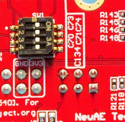
The switches in the "off" state will isolate the FTDI and allow you to use an external JTAG probe (such as Xilinx Platform Cable USB II).
USB rules for Linux
To allow openFPGAloader to program our device, add the following rules:
sudo su
cat <<EOF > /etc/udev/rules.d/99-openfpgaloader.rules
# Copy this file to /etc/udev/rules.d/

ACTION!="add|change", GOTO="openfpgaloader_rules_end"

# gpiochip subsystem
SUBSYSTEM=="gpio", MODE="0664", GROUP="plugdev", TAG+="uaccess"

SUBSYSTEM!="usb|tty|hidraw", GOTO="openfpgaloader_rules_end"

# Original FT232/FT245 VID:PID
ATTRS{idVendor}=="0403", ATTRS{idProduct}=="6001", MODE="664", GROUP="plugdev", TAG+="uaccess"

# Original FT2232 VID:PID
ATTRS{idVendor}=="0403", ATTRS{idProduct}=="6010", MODE="664", GROUP="plugdev", TAG+="uaccess"

# Original FT4232 VID:PID
ATTRS{idVendor}=="0403", ATTRS{idProduct}=="6011", MODE="664", GROUP="plugdev", TAG+="uaccess"

# Original FT232H VID:PID
ATTRS{idVendor}=="0403", ATTRS{idProduct}=="6014", MODE="664", GROUP="plugdev", TAG+="uaccess"

# Original FT231X VID:PID
ATTRS{idVendor}=="0403", ATTRS{idProduct}=="6015", MODE="664", GROUP="plugdev", TAG+="uaccess"

# anlogic cable
ATTRS{idVendor}=="0547", ATTRS{idProduct}=="1002", MODE="664", GROUP="plugdev", TAG+="uaccess"

# altera usb-blaster
ATTRS{idVendor}=="09fb", ATTRS{idProduct}=="6001", MODE="664", GROUP="plugdev", TAG+="uaccess"
ATTRS{idVendor}=="09fb", ATTRS{idProduct}=="6002", MODE="664", GROUP="plugdev", TAG+="uaccess"
ATTRS{idVendor}=="09fb", ATTRS{idProduct}=="6003", MODE="664", GROUP="plugdev", TAG+="uaccess"

# altera usb-blasterII - uninitialized
ATTRS{idVendor}=="09fb", ATTRS{idProduct}=="6810", MODE="664", GROUP="plugdev", TAG+="uaccess"
# altera usb-blasterII - initialized
ATTRS{idVendor}=="09fb", ATTRS{idProduct}=="6010", MODE="664", GROUP="plugdev", TAG+="uaccess"

# dirtyJTAG
ATTRS{idVendor}=="1209", ATTRS{idProduct}=="c0ca", MODE="664", GROUP="plugdev", TAG+="uaccess"

# Jlink
ATTRS{idVendor}=="1366", ATTRS{idProduct}=="0105", MODE="664", GROUP="plugdev", TAG+="uaccess"

# NXP LPC-Link2
ATTRS{idVendor}=="1fc9", ATTRS{idProduct}=="0090", MODE="664", GROUP="plugdev", TAG+="uaccess"

# NXP ARM mbed
ATTRS{idVendor}=="0d28", ATTRS{idProduct}=="0204", MODE="664", GROUP="plugdev", TAG+="uaccess"

# icebreaker bitsy
ATTRS{idVendor}=="1d50", ATTRS{idProduct}=="6146", MODE="664", GROUP="plugdev", TAG+="uaccess"

# orbtrace-mini dfu
ATTRS{idVendor}=="1209", ATTRS{idProduct}=="3442", MODE="664", GROUP="plugdev", TAG+="uaccess"

LABEL="openfpgaloader_rules_end"

EOF

exit
Run the following to reload the rules:
sudo udevadm control --reload-rules
sudo udevadm trigger
Add user to plugdev group:
sudo usermod -a $USER -G plugdev
Programming with openFPGALoader (Linux/MacOS)
Programming the FPGA:
openFPGALoader -c ft4232 build/lowrisc_sonata_system_0/synth-vivado/lowrisc_sonata_system_0.bit
You can also check if the flag --read-register STAT is available (newer than 0.12.2 is needed) which will print detailed information about the configuration status with a recent version of openFPGALoader. This is especially helpful if you are trying to understand why the DONE LED is not coming on:
$ openFPGALoader -c ft4232 build/lowrisc_sonata_system_0/synth-vivado/lowrisc_sonata_system_0.bit --read-register STAT

CRC Error      No CRC error
Part Secured   0
MMCM lock      1
DCI match      1
EOS            0
GTS CFG B      0
GWE            0
GHIGH B        0
MODE           7
INIT Complete  1
INIT B         0
Release Done   0
Done           0
ID Error       ID error
DEC Error      0
XADC Over temp 0
STARTUP State  0
Reserved       0
BUS Width      x1
Reserved       8
In this example there is an ID error that means the wrong bitstream was used (e.g., built for an A35, A75, or A100 and not for the A50).
Vivado (Windows)
The FTDI on the board is setup to work with Vivado, and should be detected on a recent version of Vivado (tested with 2023.2), older versions will not work. It also doesn't seem to currently work on Linux, although it "should" be supported according to Xilinx.
Reloading the FTDI Chip
The FT4232H on the board needs to be programmed by Vivado to work within Vivado. This is done from the TCL Console within Vivado.
With a blank FTDI chip, you would run the command:
program_ftdi -write -ftdi=FT4232H -serial LNXXXX -board "Sonata"
Where LNXXXX is the serial number on the sticker of the board (the serial number is optional, but with a serial number set the related
COM ports will always come up on Windows with the same COM port number, which can be helpful).
This will fail if the FTDI chip was programmed before. If you need to erase an FTDI chip, you would run the command:
program_ftdi -erase
The
program_ftdicommand can also be run from the system command prompt with the Vivado path setup.
Using nix
Alternatively, you can use the nix command to load the bitstream.
nix run .#bitstream-load
JTAG Programming Using External Probe
If using an external probe, you need to connect to P10, labeled FPGA JTAG. This is normally done with flying wire leads.
Be sure you set all of the 4-position DIP switches within SW1 to OFF on the bottom of the board, otherwise your external JTAG probe will be fighting with the FTDI lines. This will cause unreliable operation.
Simulation
The Sonata simulation environment uses Verilator.
Building
Use the following command to build the simulator binary.
The resulting executable will be available at ./result/bin/sonata-simulator.
nix build .#sonata-simulator
If you'd like more control over the build, you can manually invoke FuseSoC with the following.
The resulting executable can be found at ./build/lowrisc_sonata_system_0/sim-verilator/Vtop_verilator.
NUM_CORES=4
fusesoc --cores-root=. run \
  --target=sim --tool=verilator --setup \
  --build lowrisc:sonata:system \
  --verilator_options="-j $NUM_CORES" \
  --make_options="-j $NUM_CORES"
To enable tracing append, --verilator_options='+define+RVFI' to the command above.
Notes on building natively
This is only for advanced users.
If for some reason you do not want to use the nix environment and need to set up your own environment, here are some commands that you can use if you're running using podman or Docker:
# Download LLVM toolchain
FROM ubuntu:24.04 as llvm-download
RUN apt update && apt install -y curl unzip
RUN curl -O https://api.cirrus-ci.com/v1/artifact/github/CHERIoT-Platform/llvm-project/Build%20and%20upload%20artefact%20$(uname -p)/binaries.zip
RUN unzip binaries.zip

# Build Verilator
FROM ubuntu:24.04 AS verilator-build
# Verilator dependencies
RUN apt update && apt install -y git help2man perl python3 make g++ libfl2 libfl-dev zlib1g zlib1g-dev autoconf flex bison
WORKDIR /
# Build Verilator
RUN git clone https://github.com/verilator/verilator
WORKDIR verilator
RUN git checkout v5.024
RUN mkdir install
RUN autoconf \
    && ./configure --prefix=/verilator/install \
    && make -j `nproc` \
    && make install

# Build Sonata simulator
FROM ubuntu:24.04 as sonata-build
# Sonata dependencies
RUN apt update && apt install -y git python3 python3-venv build-essential libelf-dev libxml2-dev
# Install LLVM for sim boot stub.
RUN mkdir -p /cheriot-tools/bin
COPY --from=llvm-download "/Build/install/bin/clang-13" "/Build/install/bin/lld" "/Build/install/bin/llvm-objcopy" "/Build/install/bin/llvm-objdump" "/Build/install/bin/clangd" "/Build/install/bin/clang-format" "/Build/install/bin/clang-tidy" /cheriot-tools/bin/
# Create the LLVM tool symlinks.
RUN cd /cheriot-tools/bin \
    && ln -s clang-13 clang \
    && ln -s clang clang++ \
    && ln -s lld ld.lld \
    && ln -s llvm-objcopy objcopy \
    && ln -s llvm-objdump objdump \
    && chmod +x *
COPY --from=verilator-build "/verilator/install" /verilator
WORKDIR /
# Build Sonata simulator
RUN git clone https://github.com/lowRISC/sonata-system
WORKDIR sonata-system
RUN python3 -m venv .venv \
    && . .venv/bin/activate \
    && pip install -r python-requirements.txt \
    && export PATH=/verilator/bin:$PATH \
    && fusesoc --cores-root=. run --target=sim --tool=verilator --setup --build lowrisc:sonata:system
RUN cp build/lowrisc_sonata_system_0/sim-verilator/Vtop_verilator /sonata_simulator
# Build Sonata simulator boot stub
WORKDIR sw/cheri/sim_boot_stub
RUN export PATH=/cheriot-tools/bin:$PATH \
    && make
RUN cp sim_boot_stub /sonata_simulator_boot_stub
Running baremetal
Running the simulator can be accomplished with the following command, where you can change the meminit argument to a different program if you wish:
./build/lowrisc_sonata_system_0/sim-verilator/Vtop_verilator -t --meminit=ram,./sw/cheri/cheri_sanity/boot.elf
I recommend that you make the following change to the sanity check to see quicker changes in simulation:
diff --git a/sw/cheri/cheri_sanity/boot.cc b/sw/cheri/cheri_sanity/boot.cc
index 547abb3..7f7781d 100644
--- a/sw/cheri/cheri_sanity/boot.cc
+++ b/sw/cheri/cheri_sanity/boot.cc
@@ -32,7 +32,7 @@ extern "C" uint32_t rom_loader_entry(void *rwRoot)
        uint32_t switchValue = 0;
        while (true) {
                gpioValue ^= GPIO_VALUE;
-               for (int i = 0; i < 5000000; i++) {
+               for (int i = 0; i < 5; i++) {
                        switchValue = *((volatile uint32_t *) gpi);
                        switchValue <<= 4; // shift input onto LEDs and skipping LCD pins
                        *((volatile uint32_t *) gpo) = gpioValue ^ switchValue;
Running with boot stub
The Sonata software repository assumes you have a boot loader that jumps to 0x00101000.
To help with this we have a sim_boot_stub, which you can build as follows assuming you have access to CHERIoT LLVM:
make -C sw/cheri/sim_boot_stub
You can then run your example code through the simulator as follows:
./build/lowrisc_sonata_system_0/sim-verilator/Vtop_verilator -t -E sw/cheri/sim_boot_stub/sim_boot_stub -E /path/to/sonata-software/build/cheriot/cheriot/release/sonata_simple_demo
Debugging
If you want to look at the internal design in more details, you can explore the waveforms produced by the simulation using GTKWave:
gtkwave sim.fst data/pc_and_gpo.gtkw
Building Documentation
The documentation uses mdBook see the installation guide for further details on installation.
Once mdBook is installed the documentation can be built and viewed with:
mdbook serve --open
# Avoid FuseSoC using copied files in the book directory
touch book/FUSESOC_IGNORE
The second line can be ignored if you aren't building the FPGA bitstream (which uses fusesoc).
Windows Quick-Start
On Windows the easiest installation method is to copy the precompiled mdbook.exe available as a release on the previous link to the sonata-system root directory.
./mdbook.exe serve --open
Sonata release procedures
This document describes the process of creating a Sonata release. It is mostly meant for lowRISC developers who are making a release, but it is useful to make this public for transparency reasons and possibly if others are having trouble with a release. You'll need a copy of Vivado. Vivado version v2024.1 must be used for release creation and sign-off. It can be obtained from the from the Vivado Archive.
Hardware
Get the appropriate released version of the rp2040 firmware UF2, and load it on to the board.
To load it on the board: unplug Sonata, hold SW9 while replugging, then drag the UF2 file you downloaded onto the RPI-RP2 drive.
Setup release working area and check out fresh repository:
mkdir sonata-release
cd sonata-release
git clone https://github.com/lowRISC/sonata-system
cd sonata-system
git checkout $SONATA_SYSTEM_RELEASE_SHA
Build the bare-metal software including the bootloader:
nix develop .
cmake -B sw/cheri/build -S sw/cheri
cmake --build sw/cheri/build
Run the synthesis:
fusesoc --cores-root=. run --target=synth --setup --build lowrisc:sonata:system
Open Vivado GUI:
make -C build/lowrisc_sonata_system_0/synth-vivado build-gui
Check the following:
- No timing failures (positive or 0 wns)
- Synthesis and implementation errors (see known errors below)
- Critical warnings (see known critical warnings below)
Create UF2 (alter output filename to have correct version number in place of X.Y):
uf2conv -b 0x00000000 -f 0x6ce29e6b build/lowrisc_sonata_system_0/synth-vivado/lowrisc_sonata_system_0.bit -co sonata-vX.Y.bit.slot1.uf2
uf2conv -b 0x10000000 -f 0x6ce29e6b build/lowrisc_sonata_system_0/synth-vivado/lowrisc_sonata_system_0.bit -co sonata-vX.Y.bit.slot2.uf2
uf2conv -b 0x20000000 -f 0x6ce29e6b build/lowrisc_sonata_system_0/synth-vivado/lowrisc_sonata_system_0.bit -co sonata-vX.Y.bit.slot3.uf2
# Copy bitstream UF2 to parent release dir
cp sonata-vX.Y.bit.slot1.uf2 ..
cp sonata-vX.Y.bit.slot2.uf2 ..
cp sonata-vX.Y.bit.slot3.uf2 ..
Vivado - Known errors
None at the moment.
Vivado - Known critical warnings
None at the moment.
Automated testing
Run tests on simulation (note python3.11 or above required). FPGA testing is currently done in CI and requires quite a few add-ons to your board.
test_runner external connections:
- microSD card slot (SD1) -> microSD card with formatting & contents as specified by sdcard_tests.hh.
- Loopback connections
- mikroBUS (P7) MB10 "PWM" pin -> PMOD0 pin 1/IO1 (top-row, 6th from left)
- mikroBUS (P6) MB3 "CIPO" pin -> mikroBUS (P6) MB4 "COPI" pin
- mikroBUS (P7) MB8 "RX" pin -> mikroBUS (P7) MB7 "TX" pin
- Arduino (P4) "D0" -> Arduino (P4) "D1"
- Arduino (P4) "D8" -> Arduino (P4) "D9"
- PMOD0 pin 8/IO6 (bottom-row, 5th from left) -> PMOD0 pin 10/IO8 (bottom-row, 3rd from left)
- UART header (P12) TX0 -> UART header (P12) RXC
- Raspberry Pi Header (P3) -> Raspberry Pi Sense HAT
- qwiic1 (J7) -> Sparkfun AS6212 temperature sensor module
- PMOD1 -> Digilent PmodSF3 SPI flash module
- User USB -> USB type-A port of any USB Host
- Main USB -> a USB port of your computer

Run tests in Verilator sim.
# Build the simulator
fusesoc --cores-root=. run --target=sim --tool=verilator --setup --build lowrisc:sonata:system
# Run the tests
util/test_runner.py sim -e sw/cheri/build/tests/test_runner --simulator-binary build/lowrisc_sonata_system_0/sim-verilator/Vtop_verilator
Run tests on FPGA (note python3.11 or above required), adjust the /dev part to the UART as required. You will need to connect a Raspberry Pi sense HAT and a temperature sensor to QWIIC 1.
util/test_runner.py fpga -e sw/cheri/build/tests/test_runner -t util/sonata-openocd-cfg.tcl /dev/ttyUSB2
Bare-metal testing
CHERI Sanity:
util/mem_helper.sh load_program -e sw/cheri/build/checks/cheri_sanity
You should see the user LEDs flashing, then press the joystick to see them flicker.
RGB LED test:
util/mem_helper.sh load_program -e sw/cheri/build/checks/rgbled_test
Check the RGB LEDs turn on and change color in this sequence: green+red, blue+green, red+blue, off+off.
Run SPI flash test:
util/mem_helper.sh load_program -e sw/cheri/build/checks/spi_test
Open UART output:
screen /dev/ttyUSB2 921600
# Alternatively you can use picocom
picocom /dev/ttyUSB2 -b 921600 --imap lfcrlf
Output from UART:
JEDEC ID: ef 40 19
Got first flash read:
00 01 02 03 04 05 06 07 08 09 0a 0b 0c 0d 0e 0f 10 11 12 13 14 15 16 17 18 19 1a 1b 1c 1d 1e 1f 20 21 22 23 24 25 26 27 28 29 2a 2b 2c 2d 2e 2f 30 31 32 33 34 35 36 37 38 39 3a 3b 3c 3d 3e 3f 40 41 42 43 44 45 46 47 48 49 4a 4b 4c 4d 4e 4f 50 51 52 53 54 55 56 57 58 59 5a 5b 5c 5d 5e 5f 60 61 62 63 64 65 66 67 68 69 6a 6b 6c 6d 6e 6f 70 71 72 73 74 75 76 77 78 79 7a 7b 7c 7d 7e 7f 80 81 82 83 84 85 86 87 88 89 8a 8b 8c 8d 8e 8f 90 91 92 93 94 95 96 97 98 99 9a 9b 9c 9d 9e 9f a0 a1 a2 a3 a4 a5 a6 a7 a8 a9 aa ab ac ad ae af b0 b1 b2 b3 b4 b5 b6 b7 b8 b9 ba bb bc bd be bf c0 c1 c2 c3 c4 c5 c6 c7 c8 c9 ca cb cc cd ce cf d0 d1 d2 d3 d4 d5 d6 d7 d8 d9 da db dc dd de df e0 e1 e2 e3 e4 e5 e6 e7 e8 e9 ea eb ec ed ee ef f0 f1 f2 f3 f4 f5 f6 f7 f8 f9 fa fb fc fd fe ff
Got second flash read:
80 81 82 83 84 85 86 87 88 89 8a 8b 8c 8d 8e 8f 90 91 92 93 94 95 96 97 98 99 9a 9b 9c 9d 9e 9f a0 a1 a2 a3 a4 a5 a6 a7 a8 a9 aa ab ac ad ae af b0 b1 b2 b3 b4 b5 b6 b7 b8 b9 ba bb bc bd be bf c0 c1 c2 c3 c4 c5 c6 c7 c8 c9 ca cb cc cd ce cf d0 d1 d2 d3 d4 d5 d6 d7 d8 d9 da db dc dd de df e0 e1 e2 e3 e4 e5 e6 e7 e8 e9 ea eb ec ed ee ef f0 f1 f2 f3 f4 f5 f6 f7 f8 f9 fa fb fc fd fe ff ff ff ff ff ff ff ff ff ff ff ff ff ff ff ff ff ff ff ff ff ff ff ff ff ff ff ff ff ff ff ff ff ff ff ff ff ff ff ff ff ff ff ff ff ff ff ff ff ff ff ff ff ff ff ff ff ff ff ff ff ff ff ff ff ff ff ff ff ff ff ff ff ff ff ff ff ff ff ff ff ff ff ff ff ff ff ff ff ff ff ff ff ff ff ff ff ff ff ff ff ff ff ff ff ff ff ff ff ff ff ff ff ff ff ff ff ff ff ff ff ff ff ff ff ff ff ff ff
Run LCD test:
util/mem_helper.sh load_program -e sw/cheri/build/checks/lcd_check
Check the LCD displays a bouncing lowRISC logo and that the red background extends all the way to the edges.
Check the UART output is:
LCD check
need_offset: NO
or
LCD check
need_offset: YES
Run the USB connection test:
util/mem_helper.sh load_program -e sw/cheri/build/checks/usbdev_check
Connect the user USB to a laptop's USB-A port. The UART should show this:
Initialising USB
Connected
Test passed; disconnected from USB.
Run the USB echo test. First you need to apply the following diff:
diff --git a/sw/cheri/checks/usbdev_check.cc b/sw/cheri/checks/usbdev_check.cc
index 4212ae7..7c68507 100644
--- a/sw/cheri/checks/usbdev_check.cc
+++ b/sw/cheri/checks/usbdev_check.cc
@@ -26,7 +26,7 @@ using namespace CHERI;
 // - if disconnection is not enabled then a terminator emulator may be attached to `/dev/ttyUSB<n>`
 //   and a sign-on message should be observed. Any characters entered into the terminal will
 //   be echoed on the UART output.
-static constexpr bool do_disconnect = true;
+static constexpr bool do_disconnect = false;

 static void write_strn(UartPtr uart, const char *str, size_t len) {
   while (len-- > 0u) {
Then use the following commands:
cmake --build sw/cheri/build
util/mem_helper.sh load_program -e sw/cheri/build/checks/usbdev_check
Check the UART output is:
Initialising USB
Connected
Sent sign-on message over USB.
Open USB serial output.
For me this is screen /dev/ttyUSB1.
Check that the output is:
Hello from CHERI USB!
Also type into the USB screen instance and see that it is echoed on the UART side.
Here are some checks that you should also do for which there are no detailed instructions:
- Check the manual pinmux test over PMOD.
- Check the RS-485 is working.
Software repository
Check out fresh software repository:
cd ..
git clone https://github.com/lowRISC/sonata-software
cd sonata-software
git checkout $SONATA_SOFTWARE_RELEASE_SHA
git submodule update --init --recursive
Run through the instructions on the Sonata software getting started page. This must work with the latest release. In particular we need these commands to work:
nix develop .
xmake -P examples
Simple demo
Load simple demo on to board and make a copy for release:
# Copy for the release
cp build/cheriot/cheriot/release/sonata_simple_demo.slot1.uf2  ../sonata_simple_demo_vX.Y.slot1.uf2
# Program onto the FPGA
cp ../sonata_simple_demo_vX.Y.slot1.uf2 /media/$USER/SONATA
The LCD should display a lowRISC logo, 'Running on Sonata!' at the top and 'protected by CHERI' at the bottom. The user LEDs should display a walking pattern.
Open screen:
screen /dev/ttyUSB2 921600
You should see output from the simple demo after you press the reset button (SW5). The git SHA will depend on the commit your built your bitstream on, please confirm this is the same as you expect.
bootloader: Sonata system git SHA: 9f794fe3bd4eec8d
bootloader: Selected software slot: 1
bootloader: Loading software from flash...
bootloader: Booting into program, hopefully.
Led Walk Raw: Look pretty LEDs!
Proximity test
Load proximity sensor demo on to board
cp build/cheriot/cheriot/release/sonata_proximity_demo.slot3.uf2 /media/$USER/SONATA
Ensure you have an APDS-9960 prox/gesture/color sensor plugged into qwiic0 and that the SW App is set to position 3.
Check this has the same visual (LEDs and LCD) behaviour as the simple demo. Wave your hand over the proximity sensor, you should see the RGB LEDs fade up and down (one on the left is red, one on the right is green) as you move your hand. Red should fade up as your hand gets closer, green should fade down. Check that the RGB LED colours are as expected. This helps catch any issues that mix up the R,G,B values.
Look at the UART output:
screen /dev/ttyUSB2 921600
You should see output from the proximity demo:
proximity sensor example: Proximity is 0x12
proximity sensor example: Proximity is 0x11
proximity sensor example: Proximity is 0x16
proximity sensor example: Proximity is 0x19
proximity sensor example: Proximity is 0x1a
proximity sensor example: Proximity is 0x1c
proximity sensor example: Proximity is 0x1c
proximity sensor example: Proximity is 0x1a
proximity sensor example: Proximity is 0x18
These values will change as you move your hand over the proximity sensor.
Snake demo
Load snake demo, set your software switch to 2 and play snake:
# Copy to parent release dir
cp build/cheriot/cheriot/release/snake_demo.slot2.uf2  ../snake_demo_vX.Y.slot2.uf2
# Program onto the FPGA
cp ../snake_demo_vX.Y.slot2.uf2 /media/$USER/SONATA/
Check that you see capability the exception LEDs light up and fade out when you hit the game boundaries ('tag' exception for top and left boundaries, 'bounds' exception for bottom and right boundaries).
Also, check the UART output and check that the screen resolution matches that of the board you are testing on:
bootloader: Selected software slot: 2
bootloader: Loading software from flash...
bootloader: Booting into program, hopefully.
Snake: Detected display resolution: 160 128
Snake: Calculated game size based on settings: 12x10
RTOS test suite
Run and build the CHERIoT RTOS test suite, make sure to switch the software app to position 3:
rm -r build .xmake
xmake config -P cheriot-rtos/tests/ --board=sonata-1.1
xmake -P cheriot-rtos/tests/
llvm-strip build/cheriot/cheriot/release/test-suite -o test-suite.strip
uf2conv -b 0x20000000 -f 0x6ce29e60 test-suite.strip -co test-suite.slot3.uf2
cp test-suite.slot3.uf2 /media/$USER/SONATA
Results are output on the terminal (see instructions above), you will want to open that before you run the test suite otherwise you may miss it!
A successful run will output a large amount of text, it ends with something like:
Allocator test: fuzz i=0x0
Allocator test: fuzz i=0x8
Allocator test: fuzz i=0x10
Allocator test: fuzz i=0x18
Allocator test: fuzz i=0x20
Allocator test: fuzz i=0x28
Allocator test: fuzz i=0x30
Allocator test: fuzz i=0x38
Test runner: Allocator finished in 30477954 cycles
Test runner: All tests finished in 42895559 cycles
Also, as you run the test suite, you should see all the error LEDs light up except for execute permission, stoe local capability permission and access system register permission.
Ethernet
While staying inside the Sonata Software Nix environment take a copy of the CHERIoT platform demo repository which contains a copy of the RTOS and the network stack:
cd ..
git clone --recursive https://github.com/CHERIoT-Platform/cheriot-demos.git
cd cheriot-demos
xmake config -P network-stack/examples/01.SNTP --board=sonata-1.1 --IPv6=false
xmake -P network-stack/examples/01.SNTP
cp build/cheriot/cheriot/release/01.sntp_example sntp_example.elf
llvm-strip sntp_example.elf -o sntp_example_stripped.elf
uf2conv -b 0x00000000 -f 0x6ce29e60 sntp_example_stripped.elf -co sntp_example_stripped_elf.slot1.uf2
cp sntp_example_stripped_elf.slot1.uf2 /media/$USER/SONATA
You should then connect using Picocom and check the UART output looks something like:
bootloader: Sonata system git SHA: b833c7ab8aa4807f
bootloader: Selected software slot: 1
bootloader: Loading software from flash...
bootloader: Booting into program, hopefully.
Network test: Updating NTP took 0x7 ticks
Network test: Current UNIX epoch time: 1746630223
...
You can also check the more complicated MQTT example:
xmake config -P network-stack/examples/01.SNTP --board=sonata-1.1 --IPv6=false
xmake -P network-stack/examples/04.MQTT
cp build/cheriot/cheriot/release/04.mqtt_example mqtt_example.elf
llvm-strip mqtt_example.elf -o mqtt_example_stripped.elf
uf2conv -b 0x00000000 -f 0x6ce29e60 mqtt_example_stripped.elf -co mqtt_example_stripped_elf.slot1.uf2
cp mqtt_example_stripped_elf.slot1.uf2 /media/$USER/SONATA
You should see the following UART:
bootloader: Sonata system git SHA: b833c7ab8aa4807f
bootloader: Selected software slot: 1
bootloader: Loading software from flash...
bootloader: Booting into program, hopefully.
MQTT example: Updating NTP took 0x5 ticks
MQTT example: Current UNIX epoch time: 1746630869
MQTT example: Generating client ID...
MQTT example: Connecting to MQTT broker...
MQTT example: Connected to MQTT broker!
MQTT example: Subscribing to test topic 'cherries'.
MQTT example: Now fetching the SUBACK.
MQTT example: Got an ACK for packet 0x1
MQTT example: Publishing a value to test topic 'cherries'.
MQTT example: Now fetching the PUBACK and waiting for the publish notification.
MQTT example: Got a PUBLISH for topic cherries
MQTT example: Got an ACK for packet 0x2
MQTT example: Unsubscribing from topic 'cherries'.
MQTT example: Got an ACK for packet 0x3
MQTT example: Disconnecting from the broker.
MQTT example: Now checking for leaks.
MQTT example: No leaks detected.
MQTT example: Done testing MQTT.
While testing the ethernet, I had to connect the Sonata board directly to a router that had internet connectivity. Occasionally I had to disconnect the ethernet cable and reset the board a few times.
Make Release
In your release directory from the procedures above you should have:
sonata-vX.Y.bit.slot1.uf2sonata-vX.Y.bit.slot2.uf2sonata-vX.Y.bit.slot3.uf2sonata_simple_demo_vX.Y.slot1.uf2snake_demo_vX.Y.slot2.uf2
Use these to create the GitHub release, remember to include the RP2040 UF2 and include appropriate release notes.
Versioning
Choose a release number in the form "vX.Y" which is higher than the previous release. Create a tag in sonata-system:
# Create git tag
git tag vX.Y
# Push this tag to upstream
git push --set-upstream origin vX.Y
For the sonata-software repository we should create a branch:
git checkout -b vX.Y
git push --set-upstream origin vX.Y
Release notes
Look for the previous tagged release and go through the commit history since then. Note down any major updates like the additions of an IP block and make a bulleted list. In Vivado look for the utilization report of the placed design, the timing summary of the routed design and the power report of the routed design to fill in the bitstream characteristics. An example release notes looks something like this:
Please use the [vX.Y branch of the sonata software repository](https://github.com/lowRISC/sonata-software/tree/vX.Y) for compatible software.

## Release Notes

This release contains on top of PREVIOUS_RELEASE:
- MAJOR_FEATURE_ADDED_1
- MAJOR_FEATURE_ADDED_2
...

## Bitstream information

The utilization of the bitstream:

| Type | Used | Available | Percentage |
|------|------|-----------|------------|
| Slice LUTs | YY,YYY | 32,600 | XX.XX% |
| Slice Registers | YY,YYY | 65,200 | XX.XX% |
| Block RAM Tiles | YY | 75 | XX.XX% |
| DSPs | YY | 120 | XX.XX% |

Other bitstream statistics:

| Name | Value |
|------|-------|
| Overall WNS | Y.YYY ns |
| System clock WNS | Y.YYY ns |
| HyperRAM clock WNS | Y.YYY ns |
| USB clock WNS | Y.YYY ns |
| Total on-chip power | Y.YYY W |

## Quick start guide

Here's the developer flow for using these files:

1. Make sure the bitstream select switch (immediately below the main USB-C port) is set to position 1.
2. Before plugging in your Sonata board, hold down the "SW9" button labelled "RP2040 Boot", and while holding this button plug your board into your laptop using the Main USB.
3. A drive called "RPI-RP2" should pop up on your computer and copy rpi_rp2_vX.Y.uf2 into it.
4. This drive should automatically dismount once the file is transferred and remount as "SONATA". Once the remount has happened, you can drag in the wrapped bitstream sonata_bitstream_vX.Y.bit.slot1.uf2.
5. Once programming is successful, you should see the "CHERI" LED light up and the "LEGACY" LED turn off. If this is not the case, the bitstream loading may have failed and you should retry by unplugging and replugging the main USB on the Sonata board. Then re-drag the bitstream into the "SONATA" drive.
6. After programming the bitstream, drag the sonata_simple_demo_vX.Y.slot1.uf2 into the "SONATA" drive.
7. You should now see the user LEDs turn on and off, as well as the lowRISC logo appear on the LCD.
8. You can also drag snake_demo_vX.Y.slot2.uf2 into the SONATA drive to play snake using the joystick. Make sure to switch to the second software slot (SW7) and reset the board with SW5. Watch the CHERI error LEDs as you hit the boundary.
Setting up SD card image for 'sdcard_tests.hh'
To set up a FAT32-formatted SD card image 'sd.img' on a Linux system, the following may be useful:
https://github.com/procount/fat32images offers various ready-to-download volume images. The 1GiB example (nnobs1gb.img.zip) should suffice; rename it to 'sd.img'
Find the offset of the FAT32 partition:
fdisk -u sd.img
Disk sd.img: 1 GiB, 1073741824 bytes, 2097152 sectors
Units: sectors of 1 * 512 = 512 bytes
Sector size (logical/physical): 512 bytes / 512 bytes
I/O size (minimum/optimal): 512 bytes / 512 bytes
Disklabel type: dos
Disk identifier: 0x6c4676d7

Device        Boot Start     End Sectors  Size Id Type
noobs1gb.img1       8192 2097151 2088960 1020M  c W95 FAT32 (LBA)
Note the 'Start' value (8192) and multiply it by the sector size (512 bytes), e.g. 4194304 in the command below:
Create a mount point within the filing system for the FAT32 partition.
mkdir mnt_point
Make the FAT32 partition available.
sudo mount -o loop,offset=4194304 mnt_point sd.img
Copy the lorem ipsum text (or other files) into the root directory of the FAT32 partition.
sudo cp
mnt_point/lorem.ips
Unmount the FAT32 partition.
sudo umount mnt_point
Sonata Hardware Reference
Sonata consists of a many layers, even just in the hardware.
At its foundation is the Sonata Board. A Printed Circuit Board (PCB) with many components and expansion ports. These are fixed and unchanging, except for possible slight changes between revisions.
The central component of the Sonata board is the Field-Programmable Gate Array (FPGA) chip. Such devices can be configured (using a "bitstream") to model a digital logic design of your choosing. In this project, we load the Sonata Core onto the FPGA. FPGAs can be configured and reconfigured any number of times, so the Sonata core can be continuously developed and loaded onto existing boards.
The following sections provide reference information for the Sonata Core and the Sonata Board.
Sonata Core Reference
In a classical microcontroller, you would have a core along with the peripherals around the core. On the Sonata system this is all part of an open-source FPGA design, which allows you to modify the core to add new features (and for us to add updates to your core without needing you to desolder your main IC!).
This also means you can customize your design. You may want to have a different number of UARTs or SPI blocks for example. This document describes the base configuration.
The FPGA image is parameterizable to enable custom setups. It should be easy, for example, to change the number of UART, SPI and I2C instances. We will provide pre-built images for common configurations.
Interoperate
For the interoperable requirement, we need to make sure our hardware design can interact with that of OpenTitan Earl Grey. Since OpenTitan Earl Grey uses a TileLink Uncached Lightweight (TL-UL) bus, we use the same in the Sonata system to ease designing a bridge interface.
Hardware IP blocks
To support all the peripherals that are on the FPGA boards, we need corresponding hardware IP blocks for Ibex to be able to interact with them:
- I2C for QWIIC
- SPI for the LCD screen and ethernet
- GPIO for buttons and LEDs
- HyperRAM controller
There might be other IP blocks necessary for interacting with headers such as an analogue to digital converter. We also need some modifications to CHERIoT Ibex, which are detailed in its own page.
Wherever possible, we reuse existing, high-quality, open-source hardware IP blocks that are fit for purpose.
Memory layout
For all registers in this section, the functionality is mapped onto the least significant bits of registers and each register is 32 bits wide.
| Base address | Size | Functionality |
|---|---|---|
| 0x0010_0000 | 128 KiB | Internal SRAM |
| 0x3000_0000 | 2 KiB | Revocation tags |
| 0x4000_0000 | 1 MiB | Tagged HyperRAM |
| 0x4010_0000 | 7 MiB | Reserved for untagged RAM |
| 0x8000_0000 | 4 KiB | GPIO |
| 0x8000_1000 | 4 KiB | PWM |
| 0x8000_2000 | 4 KiB | Reserved for DMA |
| 0x8000_3000 | 4 KiB | Reserved |
| 0x8000_4000 | 4 KiB | Reserved |
| 0x8000_5000 | 4 KiB | Pinmux |
| 0x8000_6000 | 4 KiB | Reserved |
| 0x8000_7000 | 4 KiB | Reserved |
| 0x8000_8000 | 4 KiB | Reserved |
| 0x8000_9000 | 4 KiB | RGB LED controller |
| 0x8000_A000 | 4 KiB | Hardware revoker |
| 0x8000_B000 | 4 KiB | ADC |
| 0x8000_C000 | 4 KiB | System info |
| 0x8004_0000 | 64 KiB | Timer |
| 0x8010_0000 | 1 MiB | UART |
| 0x8020_0000 | 1 MiB | I2C host |
| 0x8030_0000 | 1 MiB | SPI host |
| 0x8040_0000 | 1 MiB | USB device |
| 0x8800_0000 | 64 MiB | PLIC |
| 0xB000_0000 | 4 KiB | Debug module |
Clocking infrastructure
The whole system is driven by the same clock with the exception of the HyperRAM controller. Optionally the HyperRAM controller can be clocked higher than the rest of the chip. To accommodate this, we introduce a synchronization interface with primitive FIFOs.
Memory architecture
We have a few different types of memory in the Sonata system: FPGA SRAM, HyperRAM and flash. With CHERI we need to think about capability tags and revocation tags. Any memory that needs to contain capabilities must have one capability tag per 32 bits. Any memory that needs to be revocable must have one revocation tag per 32 bits.
Capability tags
All of SRAM and 1 MiB of HyperRAM have corresponding capability tags. We envision code and read-only data to live in HyperRAM, while the stack and the heap live in SRAM.
Revocation tags
Revocation tags are essential in providing temporal memory safety in CHERI. This only covers a subset of memory that is likely to be used by the heap. Setting the revocation bit effectively stops any capability with that base address from being loaded from memory. This is a temporary step as the revocation engine scans through memory to invalidate all capabilities to this address. Once the complete memory is scanned, the revocation bit can be unset and the memory can be reused.
In Sonata, the revocation tags only cover a subset of mapped memory. They apply to memory regions that are most likely to be used as heap, it covers all of the internal SRAM but none of HyperRAM. Unlike capability tags, revocation tags need to be memory mapped so the memory allocator can manipulate them.
In CHERIoT Ibex the size of memory allocated for this is defined by TSMapSize which indicates how many 32-bit words can be used for revocation bits.
The default value for this is 1,024, which corresponds to 8 KiB.
In CHERIoT Safe the size of the revocation tag memory is 16 KiB.
List of SRAM blocks
Here's a list of blocks by size that we need to allocate in SRAM. The XC7A50T has 150 blocks of 18 kilobit block RAM, see datasheet. In total that gives use 337 KiB of block RAM, but we may not efficiently map onto 18 kilobit blocks and thus lose some memory. The block RAM usage in the table below was calculated using Vivado 2024.1's block memory generator:
| Type | Size | Width | Depth | RAM Blocks |
|---|---|---|---|---|
| Internal memory | 128 KiB | 33 | 32,768 | 60 |
| Revocation tags | 2 KiB | 32 | 512 | 1 |
| RAM capability tags | 36 KiB | 32 | 9,216 | 18 |
| Instruction cache data | 4 KiB | 64 | 512 | 2 |
| Instruction cache tags | 1 KiB | 22 | 512 | 1 |
| Total | 171 KiB | 82 | ||
| Available | 337 KiB | 150 |
Ibex
For details on how Ibex works please look at the vendored in documentation. This page highlights the changes that we made to Ibex for the Sonata system.
The Sonata board has a CHERI enabled LED which is hard wired to the value of cheri_pmode_i of the Ibex core module.
Capability exception LEDs
In the CHERIoT specification there are number of capability exception codes.
The Sonata board has dedicated LEDs to indicate any of these errors.
When one of these exceptions is seen, it gets latched and displayed on the LED.
The LEDs do not clear once the exception is handled, instead software needs to clear these LEDs through a special CSR.
Custom M-mode CSR 0xBC0 is used for this purpose.
If bit 0 is set to 1 then hardware no longer drives the LEDs and software is in full control over the output.
The other bits positions correspond to the value of the exception code.
| Bit offset | Description |
|---|---|
| 24 | Permit access system registers violation |
| 22 | Permit store local capability violation |
| 21 | Permit store capability violation |
| 19 | Permit store violation |
| 18 | Permit load violation |
| 17 | Permit execute violation |
| 3 | Seal violation |
| 2 | Tag violation |
| 1 | Bounds violation |
| 0 | Disable |
GPIO
The General Purpose Input and Output (GPIO) sub-system provides a generic low-speed means of interacting with components outside of the FPGA. Multiple GPIO instances are provided in an array within the GPIO sub-system. The first GPIO instance allows Ibex to sense the state of the on-board buttons/switches and to drive the on-board LEDs. Further GPIO instances are provided for the GPIO pins of the various on-board expansion headers. Pin-Change INTerrupt (PCINT) logic allows interrupts to be generated from external stimuli.
Note that the PCINT capture logic is not asynchronous. A pin must change for at least one system-clock cycle (default 40 MHz) to be detected.
Registers
Each instance has its own self-contained set of registers to aid compartmentalisation.
Most of the registers within most instances share an instance-specific mapping between register bits and external pins. The common case is where the same pins are used for both input or output, and for register bits to each represent pins. The exceptions are the on-board peripherals GPIO instance, and the control and status registers. Both of these kinds of special case are covered further below.
Output & Output Enable Registers
Pins can be driven as outputs by setting matching bits in the output enable register and writing the desired value to the output register. When writing, it only writes the bits for which the output is set to enable. When the output enable is set to zero it instead acts as an input pin.
The input and output registers have the same bit mapping for all but the on-board peripherals GPIO instance.
Input & Debounced Input Registers
Each GPIO instance provides debounced input values as well as raw (pre-debouncing) values in separate registers. Debouncing is useful when using mechanical switches to avoid counting a single button press multiple times. For more information on why this is, see the Wikipedia page on contact bounce. Debouncing is performed by checking that any change on an input pin remains stable throughout at least one cycle of a shared hardware timer before the change is propagated to the register. The alternative 'raw' input register is provided for situations where more precise timing is required.
Control & Status Registers
The control register and the status register are the only registers where each bit is not mapped to a physical pin.
The control register is currently only used for PCINT functionality.
| Bit offset | Description |
|---|---|
| 31 | PCINT instance-wide enable; does not affect the operation of the status register. |
| 30-4 | Reserved |
| 3 | PCINT debounced input select: 0=raw-input, 1=debounced-input. |
| 2 | Reserved |
| 1-0 | PCINT mode: 0=any-edge, 1=rising-edge, 2=falling-edge, 3=low-level. |
The status register is currently only used for PCINT functionality.
| Bit offset | Description |
|---|---|
| 31 | PCINT status; write 1 to clear. |
PCINT Mask Register
The PCINT mask register allows a custom subset of pins to be used for PCINT generation. Set a bit to enable monitoring and possible PCINT generation according to the state of the control and status register. Clear a bit to ignore that pin.
The input and PCINT mask registers have the same bit mapping for all GPIO instances.
Memory Map
The addresses of each register of each GPIO instance is given in the following table.
| Offset | Register |
|---|---|
| 0x0000 | On-board output |
| 0x0004 | On-board input |
| 0x0008 | On-board debounced input |
| 0x000C | On-board output enable (currently not used) |
| 0x0010 | On-board control |
| 0x0014 | On-board status |
| 0x0018 | On-board PCINT mask |
| 0x0040 | R-Pi output |
| 0x0044 | R-Pi input |
| 0x0048 | R-pi debounced input |
| 0x004C | R-pi output enable |
| 0x0050 | R-Pi control |
| 0x0054 | R-Pi status |
| 0x0058 | R-Pi PCINT mask |
| 0x0080 | Arduino output |
| 0x0084 | Arduino input |
| 0x0088 | Arduino debounced input |
| 0x008C | Arduino output enable |
| 0x0090 | Arduino Control |
| 0x0094 | Arduino status |
| 0x0098 | Arduino PCINT mask |
| 0x00C0 | PMOD0 output |
| 0x00C4 | PMOD0 input |
| 0x00C8 | PMOD0 debounced input |
| 0x00CC | PMOD0 output enable |
| 0x00D0 | PMOD0 control |
| 0x00D4 | PMOD0 status |
| 0x00D8 | PMOD0 PCINT mask |
| 0x0100 | PMOD1 output |
| 0x0104 | PMOD1 input |
| 0x0108 | PMOD1 debounced input |
| 0x010C | PMOD1 output enable |
| 0x0110 | PMOD1 control |
| 0x0114 | PMOD1 status |
| 0x0118 | PMOD1 PCINT mask |
| 0x0140 | PMODC output |
| 0x0144 | PMODC input |
| 0x0148 | PMODC debounced input |
| 0x014C | PMODC output enable |
| 0x0150 | PMODC control |
| 0x0154 | PMODC status |
| 0x0158 | PMODC PCINT mask |
Instances
There are several GPIO instances, each with its own mapping of external pins to register bits.
On-board Peripherals
Unlike most GPIO instances here, the on-board peripherals instance uses a different pin mapping for input compared to output. It interfaces with soldered-on user switches, buttons, and LEDs, for each of which only one of input or output makes sense.
The output register drives the user LEDs.
| Bit offset | Description |
|---|---|
| 7-0 | LEDs |
In this case writing a one will turn an LED on and a zero will turn the LED off.
Note: the output enable register does nothing in this instance, as the outputs are not shared with inputs.
The raw input and debounced input registers sense the state of the various user switches/buttons/joystick available on the board, and the microSD card detection line.
| Bit offset | Description |
|---|---|
| 16 | MicroSD card detection (0: present, 1: absent) |
| 15-13 | Software select switches (1, 2, 3) |
| 12-8 | Joystick (left, down, up, right, press) |
| 7-0 | DIP switches |
It is recommended to use the debounced input for these mechanical switches.
Raspberry Pi HAT
The Raspberry Pi HAT header has 28 pins that can act as GPIO. Some can be remapped to other IP blocks (see Pinmux documentation).
| Bit offset | Description |
|---|---|
| 27-0 | GPIO 27 to 0 |
Note: Before using the Raspberry Pi HAT header's GPIO you should use the pinmux to configure them as input or output.
Arduino Shield
The Arduino Shield header has 14 pins that can act as GPIO.
| Bit offset | Description |
|---|---|
| 13-0 | GPIO 13 to 0 |
Pmod
The Pmod header is split up as Pmod 0, C and 1. Pmod 0 and 1 have 8 GPIO outputs each while C has 6.
| Bit offset | Description |
|---|---|
| 7-6 | Accessible for Pmod 0 and 1 only |
| 5-0 | Accessible for Pmod 0, 1 and C |
Pulse width modulation (PWM)
Pulse width modulation allows you to create a block wave with a certain duty cycle. It is useful for use cases like dimming LEDs.
             <--> pulse-width
___          ____          ____
   |        |    |        |    |           duty-cycle = pulse-width / period
   |________|    |________|    |______
             <--period--->
There are 12 PWM channels.
Each channel consists of a free-running 8-bit counter with two configurable comparators. The period comparator resets the counter value back to zero once it reaches a user-configured top value. This sets the period (number of cycles between rising-edges of pulses) of the output waveform. The pulse width comparator changes the channel output from high to low when the counter value surpasses a user-configured pulse width value. This sets the pulse width (number of cycles the output spends high) of the output waveform.
Each channel has a 64-bit section in the address space for configuration.
| Offset | PWM channel |
|---|---|
| 0x00 | Channel 0 |
| 0x08 | Channel 1 |
| 0x10 | Channel 2 |
| 0x18 | Channel 3 |
| 0x20 | Channel 4 |
| 0x28 | Channel 5 |
| 0x30 | Channel 6 |
To see which pins can be connected to which channel please consult the pin multiplexer.
Config
For each channel, there is a 32-bit register defining the pulse width and another 32-bit register above it defining how long the complete wave is (counter top). These registers are write-only, and will return a value of zero if read. The counters are only 8-bit wide, any values written that are larger than 8-bits are invalid.
| Offset | Description | Read/Write |
|---|---|---|
| 0x0 | Pulse width | Write-only |
| 0x4 | Counter top | Write-only |
A channel is enabled by setting an non-zero counter top value.
To generate an always-low signal, set a counter top value of zero. To generate an always-high signal, set a pulse-width value greater than the (non-zero) counter top value.
HyperRAM
HyperRAM is used as an alternative to flash. Compared to flash, HyperRAM has similar performance but it avoids the need for a quad-speed SPI controller to interact with the flash. For details on the Windbond W956D8MBYA5I HyperRAM chip used on the Sonata board, see the datasheet. We anticipate mostly code to live in HyperRAM and to make sure that we don't suffer from access latency, we enable the instruction cache in Ibex.
Capability enabled RAM
Currently only 1 MiB of HyperRAM is accessible and all of that has associated capability tags, these tags are stored in 16 KiB of SRAM.
Analogue to digital converter (ADC)
The FPGA provides an analogue to digital converter called XADC, and this hardware IP block provides a memory mapped way of interacting with that. Please see the specification for XADC for a more detailed description of how it works.
Analogue Input Channels
The six Arduino shield analogue input pins (A0-A5) are connected to six of the XADC Vaux channels.
| Pin | Channel |
|---|---|
| A0 | Vaux[4] |
| A1 | Vaux[12] |
| A2 | Vaux[5] |
| A3 | Vaux[13] |
| A4 | Vaux[6] |
| A5 | Vaux[14] |
The input range at the shield pin is 0-5V. Conversion from a single-ended 0-5V signal at the shield pin to a 0-1V differential signal at the XADC inputs is handled by on-board buffering and balancing circuit. Note that impedance drops above 3.3V due to diode clamps on a resistor-gated branch that also connects each pin to a digital FPGA input (currently unused).
Sensors
A set of on-chip sensors can also be read by the XADC. The most interesting of these is a temperature sensor. The rest are various supply/reference voltages.
Registers
The XADC is accessed via its Dynamic Reconfiguration Port (DRP), which give access to various 16-bit control and status registers. These registers have been memory mapped at a 32-bit intervals to simplify accesses.
| DRP Address | Register |
|---|---|
| 0x00 0x01 .. 0x3F | Status |
| 0x40 0x41 .. 0x7F | Control |
| Memory-Mapped Offset | Register |
|---|---|
| 0x000 0x004 .. 0x0FC | Status |
| 0x100 0x104 .. 0x1FC | Control |
By default, the XADC will continuously sample all six routed analogue inputs and all on-chip sensors at a low sample rate, with conversion results ready to be read by the host from the status registers. This default configuration is achieved by specifying initial values for the configuration registers in the RTL. The sample rate or other configuration can be changed by writing to the control registers.
For a more detailed description of all of these registers please see Chapter 3 of the XADC specification.
Pin multiplexer
This allows software to dynamically switch FPGA pins between input and output as well as reassign them for SPI, I2C, UART, etc. The block also allows pad control.
To see the possible mappings, please refer to the top configuration. All selectors are byte addressable, this means that you can write four selectors at a time with a 32-bit write.
There are output pin selectors, which select which block output is connected to a particular FPGA pin.
The selector is one-hot, so you need to write 8'b100 if you want to select input 3 for example.
The default value for all of these selectors is 'b10. As a consequence, you will need to use the pinmux before attempting use the additional headers as GPIO (e.g. the Raspberry Pi header's GPIO).
| Address | Pin output | Possible block outputs |
|---|---|---|
| 0x000 | ser0_tx | 0, uart_0_tx |
| 0x001 | ser1_tx | 0, uart_1_tx, uart_2_tx |
| 0x002 | rs232_tx | 0, uart_2_tx |
| 0x003 | rs485_tx | 0, uart_2_tx |
| 0x004 | scl0 | 0, i2c_0_scl |
| 0x005 | sda0 | 0, i2c_0_sda |
| 0x006 | scl1 | 0, i2c_1_scl |
| 0x007 | sda1 | 0, i2c_1_sda |
| 0x008 | rph_g0 | 0, i2c_0_sda, gpio_0_ios_0 |
| 0x009 | rph_g1 | 0, i2c_0_scl, gpio_0_ios_1 |
| 0x00a | rph_g2_sda | 0, i2c_1_sda, gpio_0_ios_2 |
| 0x00b | rph_g3_scl | 0, i2c_1_scl, gpio_0_ios_3 |
| 0x00c | rph_g4 | 0, gpio_0_ios_4 |
| 0x00d | rph_g5 | 0, gpio_0_ios_5 |
| 0x00e | rph_g6 | 0, gpio_0_ios_6 |
| 0x00f | rph_g7 | 0, spi_1_cs_1, gpio_0_ios_7 |
| 0x010 | rph_g8 | 0, spi_1_cs_0, gpio_0_ios_8 |
| 0x011 | rph_g9 | 0, gpio_0_ios_9 |
| 0x012 | rph_g10 | 0, spi_1_copi, gpio_0_ios_10 |
| 0x013 | rph_g11 | 0, spi_1_sclk, gpio_0_ios_11 |
| 0x014 | rph_g12 | 0, gpio_0_ios_12, pwm_out_0 |
| 0x015 | rph_g13 | 0, gpio_0_ios_13, pwm_out_1 |
| 0x016 | rph_txd0 | 0, uart_1_tx, gpio_0_ios_14 |
| 0x017 | rph_rxd0 | 0, gpio_0_ios_15 |
| 0x018 | rph_g16 | 0, spi_2_cs_2, gpio_0_ios_16 |
| 0x019 | rph_g17 | 0, spi_2_cs_1, gpio_0_ios_17 |
| 0x01a | rph_g18 | 0, spi_2_cs_0, gpio_0_ios_18, pwm_out_2 |
| 0x01b | rph_g19 | 0, gpio_0_ios_19, pwm_out_3 |
| 0x01c | rph_g20 | 0, spi_2_copi, gpio_0_ios_20, pwm_out_4 |
| 0x01d | rph_g21 | 0, spi_2_sclk, gpio_0_ios_21, pwm_out_5 |
| 0x01e | rph_g22 | 0, gpio_0_ios_22 |
| 0x01f | rph_g23 | 0, gpio_0_ios_23 |
| 0x020 | rph_g24 | 0, gpio_0_ios_24 |
| 0x021 | rph_g25 | 0, gpio_0_ios_25 |
| 0x022 | rph_g26 | 0, gpio_0_ios_26 |
| 0x023 | rph_g27 | 0, gpio_0_ios_27 |
| 0x024 | ah_tmpio0 | 0, gpio_1_ios_0 |
| 0x025 | ah_tmpio1 | 0, uart_1_tx, gpio_1_ios_1 |
| 0x026 | ah_tmpio2 | 0, gpio_1_ios_2 |
| 0x027 | ah_tmpio3 | 0, gpio_1_ios_3, pwm_out_0 |
| 0x028 | ah_tmpio4 | 0, gpio_1_ios_4 |
| 0x029 | ah_tmpio5 | 0, gpio_1_ios_5, pwm_out_1 |
| 0x02a | ah_tmpio6 | 0, gpio_1_ios_6, pwm_out_2 |
| 0x02b | ah_tmpio7 | 0, gpio_1_ios_7 |
| 0x02c | ah_tmpio8 | 0, gpio_1_ios_8 |
| 0x02d | ah_tmpio9 | 0, gpio_1_ios_9, pwm_out_3 |
| 0x02e | ah_tmpio10 | 0, spi_1_cs_3, gpio_1_ios_10, pwm_out_4 |
| 0x02f | ah_tmpio11 | 0, spi_1_copi, gpio_1_ios_11, pwm_out_5 |
| 0x030 | ah_tmpio12 | 0, gpio_1_ios_12 |
| 0x031 | ah_tmpio13 | 0, spi_1_sclk, gpio_1_ios_13 |
| 0x032 | mb1 | 0, spi_2_cs_3 |
| 0x033 | mb2 | 0, spi_2_sclk |
| 0x034 | mb4 | 0, spi_2_copi |
| 0x035 | mb5 | 0, i2c_1_sda |
| 0x036 | mb6 | 0, i2c_1_scl |
| 0x037 | mb7 | 0, uart_1_tx |
| 0x038 | mb10 | 0, pwm_out_0 |
| 0x039 | pmod0_1 | 0, gpio_2_ios_0, spi_1_cs_0 |
| 0x03a | pmod0_2 | 0, gpio_2_ios_1, spi_1_copi, pwm_out_1, uart_1_tx |
| 0x03b | pmod0_3 | 0, gpio_2_ios_2, i2c_0_scl |
| 0x03c | pmod0_4 | 0, gpio_2_ios_3, spi_1_sclk, i2c_0_sda |
| 0x03d | pmod0_7 | 0, gpio_2_ios_4 |
| 0x03e | pmod0_8 | 0, gpio_2_ios_5, pwm_out_2 |
| 0x03f | pmod0_9 | 0, gpio_2_ios_6, spi_1_cs_1 |
| 0x040 | pmod0_10 | 0, gpio_2_ios_7, spi_1_cs_2 |
| 0x041 | pmod1_1 | 0, gpio_3_ios_0, spi_2_cs_0 |
| 0x042 | pmod1_2 | 0, gpio_3_ios_1, spi_2_copi, pwm_out_3, uart_2_tx |
| 0x043 | pmod1_3 | 0, gpio_3_ios_2, i2c_1_scl |
| 0x044 | pmod1_4 | 0, gpio_3_ios_3, spi_2_sclk, i2c_1_sda |
| 0x045 | pmod1_7 | 0, gpio_3_ios_4 |
| 0x046 | pmod1_8 | 0, gpio_3_ios_5, pwm_out_4 |
| 0x047 | pmod1_9 | 0, gpio_3_ios_6, spi_2_cs_1 |
| 0x048 | pmod1_10 | 0, gpio_3_ios_7, spi_2_cs_2 |
| 0x049 | pmodc_1 | 0, gpio_4_ios_0 |
| 0x04a | pmodc_2 | 0, gpio_4_ios_1 |
| 0x04b | pmodc_3 | 0, gpio_4_ios_2 |
| 0x04c | pmodc_4 | 0, gpio_4_ios_3 |
| 0x04d | pmodc_5 | 0, gpio_4_ios_4 |
| 0x04e | pmodc_6 | 0, gpio_4_ios_5 |
| 0x04f | appspi_d0 | 0, spi_0_copi |
| 0x050 | appspi_clk | 0, spi_0_sclk |
| 0x051 | appspi_cs | 0, spi_0_cs_0 |
| 0x052 | microsd_cmd | 0, spi_0_copi |
| 0x053 | microsd_clk | 0, spi_0_sclk |
| 0x054 | microsd_dat3 | 0, spi_0_cs_1 |
Besides the output pin selectors, there are also selectors for which pin should drive block inputs:
| Address | Block input | Possible pin inputs |
|---|---|---|
| 0x800 | gpio_0_ios_0 | 0, rph_g0 |
| 0x801 | gpio_0_ios_1 | 0, rph_g1 |
| 0x802 | gpio_0_ios_2 | 0, rph_g2_sda |
| 0x803 | gpio_0_ios_3 | 0, rph_g3_scl |
| 0x804 | gpio_0_ios_4 | 0, rph_g4 |
| 0x805 | gpio_0_ios_5 | 0, rph_g5 |
| 0x806 | gpio_0_ios_6 | 0, rph_g6 |
| 0x807 | gpio_0_ios_7 | 0, rph_g7 |
| 0x808 | gpio_0_ios_8 | 0, rph_g8 |
| 0x809 | gpio_0_ios_9 | 0, rph_g9 |
| 0x80a | gpio_0_ios_10 | 0, rph_g10 |
| 0x80b | gpio_0_ios_11 | 0, rph_g11 |
| 0x80c | gpio_0_ios_12 | 0, rph_g12 |
| 0x80d | gpio_0_ios_13 | 0, rph_g13 |
| 0x80e | gpio_0_ios_14 | 0, rph_txd0 |
| 0x80f | gpio_0_ios_15 | 0, rph_rxd0 |
| 0x810 | gpio_0_ios_16 | 0, rph_g16 |
| 0x811 | gpio_0_ios_17 | 0, rph_g17 |
| 0x812 | gpio_0_ios_18 | 0, rph_g18 |
| 0x813 | gpio_0_ios_19 | 0, rph_g19 |
| 0x814 | gpio_0_ios_20 | 0, rph_g20 |
| 0x815 | gpio_0_ios_21 | 0, rph_g21 |
| 0x816 | gpio_0_ios_22 | 0, rph_g22 |
| 0x817 | gpio_0_ios_23 | 0, rph_g23 |
| 0x818 | gpio_0_ios_24 | 0, rph_g24 |
| 0x819 | gpio_0_ios_25 | 0, rph_g25 |
| 0x81a | gpio_0_ios_26 | 0, rph_g26 |
| 0x81b | gpio_0_ios_27 | 0, rph_g27 |
| 0x81c | gpio_1_ios_0 | 0, ah_tmpio0 |
| 0x81d | gpio_1_ios_1 | 0, ah_tmpio1 |
| 0x81e | gpio_1_ios_2 | 0, ah_tmpio2 |
| 0x81f | gpio_1_ios_3 | 0, ah_tmpio3 |
| 0x820 | gpio_1_ios_4 | 0, ah_tmpio4 |
| 0x821 | gpio_1_ios_5 | 0, ah_tmpio5 |
| 0x822 | gpio_1_ios_6 | 0, ah_tmpio6 |
| 0x823 | gpio_1_ios_7 | 0, ah_tmpio7 |
| 0x824 | gpio_1_ios_8 | 0, ah_tmpio8 |
| 0x825 | gpio_1_ios_9 | 0, ah_tmpio9 |
| 0x826 | gpio_1_ios_10 | 0, ah_tmpio10 |
| 0x827 | gpio_1_ios_11 | 0, ah_tmpio11 |
| 0x828 | gpio_1_ios_12 | 0, ah_tmpio12 |
| 0x829 | gpio_1_ios_13 | 0, ah_tmpio13 |
| 0x82a | gpio_2_ios_0 | 0, pmod0_1 |
| 0x82b | gpio_2_ios_1 | 0, pmod0_2 |
| 0x82c | gpio_2_ios_2 | 0, pmod0_3 |
| 0x82d | gpio_2_ios_3 | 0, pmod0_4 |
| 0x82e | gpio_2_ios_4 | 0, pmod0_7 |
| 0x82f | gpio_2_ios_5 | 0, pmod0_8 |
| 0x830 | gpio_2_ios_6 | 0, pmod0_9 |
| 0x831 | gpio_2_ios_7 | 0, pmod0_10 |
| 0x832 | gpio_3_ios_0 | 0, pmod1_1 |
| 0x833 | gpio_3_ios_1 | 0, pmod1_2 |
| 0x834 | gpio_3_ios_2 | 0, pmod1_3 |
| 0x835 | gpio_3_ios_3 | 0, pmod1_4 |
| 0x836 | gpio_3_ios_4 | 0, pmod1_7 |
| 0x837 | gpio_3_ios_5 | 0, pmod1_8 |
| 0x838 | gpio_3_ios_6 | 0, pmod1_9 |
| 0x839 | gpio_3_ios_7 | 0, pmod1_10 |
| 0x83a | gpio_4_ios_0 | 0, pmodc_1 |
| 0x83b | gpio_4_ios_1 | 0, pmodc_2 |
| 0x83c | gpio_4_ios_2 | 0, pmodc_3 |
| 0x83d | gpio_4_ios_3 | 0, pmodc_4 |
| 0x83e | gpio_4_ios_4 | 0, pmodc_5 |
| 0x83f | gpio_4_ios_5 | 0, pmodc_6 |
| 0x840 | uart_0_rx | 1, ser0_rx |
| 0x841 | uart_1_rx | 1, ser1_rx, rph_rxd0, ah_tmpio0, mb8, pmod0_3 |
| 0x842 | uart_2_rx | 1, ser1_rx, rs232_rx, rs485_rx, pmod1_3 |
| 0x843 | spi_0_cipo | 0, appspi_d1, microsd_dat0 |
| 0x844 | spi_1_cipo | 0, rph_g9, ah_tmpio12, pmod0_3 |
| 0x845 | spi_2_cipo | 0, rph_g19, mb3, pmod1_3 |
Regeneration
If any changes are made to the top configuration, the templates or the bus, you must regenerate the top. You can do so using the top generation utility, which regenerates the pinmux, the bus and the sonata package which is used by the SystemVerilog generate statements throughout the project.
./util/top_gen.py
Sonata Pin Mappings

CHERIoT hardware revocation engine
This block is integrated from the CHERIoT Safe repository. It controls the hardware revoker inside CHERIoT Ibex which is the thing that does the revocation, it is looking for capabilities to freed memory. When a piece of memory is freed its revocation bits are set. The hardware revoker sweeps from the start until the end address for capabilities that point to any revoked region. For more information on how this works please refer to Section 3.3.3 (background pipelined revoker) of this paper.
These are the register offsets:
| Offset | Register |
|---|---|
| 0x0000 | Start address to begin sweeping. |
| 0x0004 | End address to stop sweeping. |
| 0x0008 | Writing any value to this register sets the hardware revoker to run. When read, the most significant byte is set to constant 0x55. |
| 0x000C | Epoch, where the last bit means a sweep is currently happening. |
| 0x0010 | Used to read interrupt status and clear it. |
| 0x0014 | Enable bit for raising an interrupt when sweeping is done. |
System information
This is a special IP block that is automatically populated with useful information about the system. These values are useful to know what the parameters were when a bitstream was generate.
| Offset | Register |
|---|---|
| 0x0000 | First 4 bytes of git commit hash from which this bistream was generated. |
| 0x0004 | Second 4 bytes of git commit hash. |
| 0x0008 | Git dirty status (1 if dirty or 0 if clean). |
| 0x000C | System clock frequency in Hz. |
| 0x0010 | GPIO info of which least significant byte is the number of instances. |
| 0x0014 | UART info of which least significant byte is the number of instances. |
| 0x0018 | I2C info of which least significant byte is the number of instances. |
| 0x001C | SPI info of which least significant byte is the number of instances. |
| 0x0020 | Initiate capture of 'DNA value' identifying the specific device. |
| 0x0024 | Next bit of the 57-bit 'DNA value' may be read in the least significant bit. |
| 0x0028 | Size of the main memory in kibibytes (KiB). |
| 0x002C | Size of the HyperRAM in kibibytes (KiB). |
| 0x0030 | Size of the tagged (capability aware) portion of the HyperRAM (KiB). |
Timer
The timer that we use in Sonata is based on the timer present in the Ibex repository. It is a simple memory mapped timer that sends an interrupt to Ibex after a specified amount of time. The time values in this block are 64 bits, which is why it has a high and a low register for each value.
| Offset | Register |
|---|---|
| 0x00 | Time low |
| 0x04 | Time high |
| 0x08 | Time compare low |
| 0x0C | Time compare high |
The processor can set the time by writing to the time low and high registers and then set a time compare value to compare to. Internally, the block increments the time by one each clock cycle. Once the internal counter has exceeded the compare value, it raises an interrupt with the Ibex.
Universal asynchronous receiver/transmitter (UART)
The Sonata system uses the OpenTitan UART. The version of the IP that is vendored in has documentation that you can find here. You can find the register definitions here.
There are multiple UART instances in Sonata to connect to any of the following targets:
- USB
- RS-232
- mikroBUS
- Arduino shield
- Raspberry Pi hat
By default, Sonata includes 3 UART blocks, each with an offset of 0x1000 from each other.
Inter-integrated circuit (I2C) host
For the I2C block in Sonata, we use the OpenTitan IP.
The version of the IP that is vendored in has documentation that you can find here.
Another useful reference is the existing driver for this block in the CHERIoT RTOS repository.
We hardcode this block to be in host mode, so you can ignore the target functionality, including the following registers: ovrd, val, target_id, acqdata and txdata.
Other than those, you can find the register definitions here.
The registers 0x00 - 0x10 are also not accessible.
The control register is just hardwired to be in host mode.
For Sonata, we include two I2C blocks.
The registers of the second I2C block can be accessed with an additional 0x1000 offset.
These can be connected to any of these I2C targets:
- Two for the QWIIC connectors.
- One for the mikroBUS.
- One for the Raspberry Pi hat.
- One for the Arduino shield.
Serial peripheral interface (SPI) host
The SPI in Sonata only has the capability to be a host. This is a simple hardware IP block that can transmit and receive bytes over SPI.
In Sonata, there are multiple uses for SPI:
- LCD screen
- Ethernet
- Flash
- MicroSD card
- Raspberry Pi HAT
- Arduino shield
- mikroBUS click
The offset for each of the blocks is shown below, with each additional block having a 0x1000 offset from the previous. The offsets in the table below are from the SPI base address, which is 0x8030_0000. The table also shows the connections of the chip select (CS) wires. CS1 for LCD and Ethernet and CS2 for LCD are not used as chip selects but rather for block specific functions like reset and data/control signals.
| Name | Offset | Blocks | CS0 | CS1 | CS2 | CS3 |
|---|---|---|---|---|---|---|
| LCD Screen | 0x0000 | Only LCD | CS | Data/control | Reset | |
| Ethernet MAC | 0x1000 | Only Ethernet | CS | Reset | ||
| SPI0 | 0x2000 | Flash or MicroSD | Flash | MicroSD | ||
| SPI1 | 0x3000 | HAT SPI0, Shield, Pmod0 | HAT or Pmod0 | HAT or Pmod0 | Pmod0 | Shield |
| SPI2 | 0x4000 | HAT SPI1, mikroBUS, Pmod1 | HAT or Pmod1 | HAT or Pmod1 | HAT or Pmod1 | mikroBUS |
Please refer to the pin multiplexer and pin mappings on how to connect SPI 0, 1 and 2.
Overview
Each SPI block has two 8-entry FIFOs - one for transmit and one for receive.
To begin an SPI transaction write to the START register.
Bytes do not need to be immediately available in the transmit FIFO nor space available in the receive FIFO to begin the transaction.
The SPI block will only run the clock when its able to proceed.
Register Table
| Name | Offset | Length | Description |
|---|---|---|---|
spi.INTR_STATE | 0x0 | 4 | Interrupt State Register |
spi.INTR_ENABLE | 0x4 | 4 | Interrupt Enable Register |
spi.INTR_TEST | 0x8 | 4 | Interrupt Test Register |
spi.CFG | 0xc | 4 | Configuration register. |
spi.CONTROL | 0x10 | 4 | Controls the operation of the SPI block. |
spi.STATUS | 0x14 | 4 | Status information about the SPI block. |
spi.START | 0x18 | 4 | When written begins an SPI operation. |
spi.RX_FIFO | 0x1c | 4 | Data from the receive FIFO. |
spi.TX_FIFO | 0x20 | 4 | Bytes written here are pushed to the transmit FIFO. |
spi.INFO | 0x24 | 4 | Returns information on the SPI controller. |
spi.CS | 0x28 | 4 | Specifies which peripherals are selected for SPI operations. |
INTR_STATE
Interrupt State Register
- Offset:
0x0 - Reset default:
0x0 - Reset mask:
0x1f
Fields
| Bits | Type | Reset | Name | Description |
|---|---|---|---|---|
| 31:5 | Reserved | |||
| 4 | rw1c | 0x0 | complete | On-going SPI operation has completed and the block is now idle |
| 3 | ro | 0x0 | tx_watermark | Transmit FIFO level is at or below watermark |
| 2 | ro | 0x0 | tx_empty | Transmit FIFO is empty |
| 1 | ro | 0x0 | rx_watermark | Receive FIFO level is at or above watermark |
| 0 | ro | 0x0 | rx_full | Receive FIFO is full |
INTR_ENABLE
Interrupt Enable Register
- Offset:
0x4 - Reset default:
0x0 - Reset mask:
0x1f
Fields
| Bits | Type | Reset | Name | Description |
|---|---|---|---|---|
| 31:5 | Reserved | |||
| 4 | rw | 0x0 | complete | Enable interrupt when INTR_STATE.complete is set. |
| 3 | rw | 0x0 | tx_watermark | Enable interrupt when INTR_STATE.tx_watermark is set. |
| 2 | rw | 0x0 | tx_empty | Enable interrupt when INTR_STATE.tx_empty is set. |
| 1 | rw | 0x0 | rx_watermark | Enable interrupt when INTR_STATE.rx_watermark is set. |
| 0 | rw | 0x0 | rx_full | Enable interrupt when INTR_STATE.rx_full is set. |
INTR_TEST
Interrupt Test Register
- Offset:
0x8 - Reset default:
0x0 - Reset mask:
0x1f
Fields
| Bits | Type | Reset | Name | Description |
|---|---|---|---|---|
| 31:5 | Reserved | |||
| 4 | wo | 0x0 | complete | Write 1 to force INTR_STATE.complete to 1. |
| 3 | wo | 0x0 | tx_watermark | Write 1 to force INTR_STATE.tx_watermark to 1. |
| 2 | wo | 0x0 | tx_empty | Write 1 to force INTR_STATE.tx_empty to 1. |
| 1 | wo | 0x0 | rx_watermark | Write 1 to force INTR_STATE.rx_watermark to 1. |
| 0 | wo | 0x0 | rx_full | Write 1 to force INTR_STATE.rx_full to 1. |
CFG
Configuration register. Controls how the SPI block transmits and receives data. This register can only be modified whilst the SPI block is idle.
- Offset:
0xc - Reset default:
0x20000000 - Reset mask:
0xe000ffff
Fields
| Bits | Type | Reset | Name |
|---|---|---|---|
| 31 | rw | 0x0 | CPOL |
| 30 | rw | 0x0 | CPHA |
| 29 | rw | 0x1 | MSB_FIRST |
| 28 | rw | 0x0 | COPI_IDLE |
| 27:16 | Reserved | ||
| 15:0 | rw | 0x0 | HALF_CLK_PERIOD |
CFG . CPOL
The polarity of the spi_clk signal. When CPOL is 0 clock is low when idle and the leading edge is positive. When CPOL is 1 clock is high when idle and the leading edge is negative
CFG . CPHA
The phase of the spi_clk signal. When CPHA is 0 data is sampled on the leading edge and changes on the trailing edge. The first data bit is immediately available before the first leading edge of the clock when transmission begins. When CPHA is 1 data is sampled on the trailing edge and change on the leading edge.
CFG . MSB_FIRST
When set the most significant bit (MSB) is the first bit sent and received with each byte.
CFG . COPI_IDLE
State of the controller output line (COPI) when not transmitting. This default state is low, but it may need to be held high for some SPI peripherals such as a (micro)SD card. The presence of 'COPI_IDLE' support may be tested by setting and then reading back this configuration bit; earlier versions of the controller returned 0 for this bit.
CFG . HALF_CLK_PERIOD
The length of a half period (i.e. positive edge to negative edge) of the SPI clock, measured in system clock cycles reduced by 1. At the standard Sonata 50 MHz system clock a value of 0 gives a 25 MHz SPI clock, a value of 1 gives a 12.5 MHz SPI clock, a value of 2 gives a 8.33 MHz SPI clock and so on.
CONTROL
Controls the operation of the SPI block. This register can only be modified whilst the SPI block is idle.
- Offset:
0x10 - Reset default:
0x0 - Reset mask:
0xfff
Fields
| Bits | Type | Reset | Name |
|---|---|---|---|
| 31:12 | Reserved | ||
| 11:8 | rw | 0x0 | RX_WATERMARK |
| 7:4 | rw | 0x0 | TX_WATERMARK |
| 3 | rw | 0x0 | RX_ENABLE |
| 2 | rw | 0x0 | TX_ENABLE |
| 1 | wo | 0x0 | RX_CLEAR |
| 0 | wo | 0x0 | TX_CLEAR |
CONTROL . RX_WATERMARK
The watermark level for the receive FIFO, depending on the value the interrupt will trigger at different points:
- 0: 1 or more items in the FIFO
- 1: 2 or more items in the FIFO
- 2: 4 or more items in the FIFO
- 3: 8 or more items in the FIFO
- 4: 16 or more items in the FIFO
- 5: 32 or more items in the FIFO
- 6: 56 or more items in the FIFO
CONTROL . TX_WATERMARK
The watermark level for the transmit FIFO, depending on the value the interrupt will trigger at different points:
- 0: 1 or fewer items in the FIFO
- 1: 2 or fewer items in the FIFO
- 2: 4 or fewer items in the FIFO
- 3: 8 or fewer items in the FIFO
- 4: 16 or fewer items in the FIFO
CONTROL . RX_ENABLE
When set incoming bits are written to the receive FIFO. When clear incoming bits are ignored.
CONTROL . TX_ENABLE
When set bytes from the transmit FIFO are sent. When clear the state of the outgoing spi_cipo is undefined whilst the SPI clock is running.
CONTROL . RX_CLEAR
Write 1 to clear the receive FIFO.
CONTROL . TX_CLEAR
Write 1 to clear the transmit FIFO.
STATUS
Status information about the SPI block
- Offset:
0x14 - Reset default:
0x0 - Reset mask:
0x7ffff
Fields
| Bits | Type | Reset | Name | Description |
|---|---|---|---|---|
| 31:19 | Reserved | |||
| 18 | ro | x | IDLE | When set the SPI block is idle and can accept a new start command. |
| 17 | ro | x | RX_FIFO_EMPTY | When set the receive FIFO is empty and any data read from it will be undefined. |
| 16 | ro | x | TX_FIFO_FULL | When set the transmit FIFO is full and any data written to it will be ignored. |
| 15:8 | ro | x | RX_FIFO_LEVEL | Number of items in the receive FIFO |
| 7:0 | ro | x | TX_FIFO_LEVEL | Number of items in the transmit FIFO |
START
When written begins an SPI operation. Writes are ignored when the SPI block is active.
- Offset:
0x18 - Reset default:
0x0 - Reset mask:
0x7ff
Fields
| Bits | Type | Reset | Name | Description |
|---|---|---|---|---|
| 31:11 | Reserved | |||
| 10:0 | wo | 0x0 | BYTE_COUNT | Number of bytes to receive/transmit in the SPI operation |
RX_FIFO
Data from the receive FIFO. When read the data is popped from the FIFO. If the FIFO is empty data read is undefined.
- Offset:
0x1c - Reset default:
0x0 - Reset mask:
0xff
Fields
| Bits | Type | Reset | Name | Description |
|---|---|---|---|---|
| 31:8 | Reserved | |||
| 7:0 | ro | x | DATA | Byte popped from the FIFO |
TX_FIFO
Bytes written here are pushed to the transmit FIFO. If the FIFO is full writes are ignored.
- Offset:
0x20 - Reset default:
0x0 - Reset mask:
0xff
Fields
| Bits | Type | Reset | Name | Description |
|---|---|---|---|---|
| 31:8 | Reserved | |||
| 7:0 | wo | 0x0 | DATA | Byte to push to the FIFO |
INFO
Returns information on the SPI controller.
- Offset:
0x24 - Reset default:
0x0 - Reset mask:
0xff
Fields
| Bits | Type | Reset | Name | Description |
|---|---|---|---|---|
| 31:16 | Reserved | |||
| 15:8 | ro | 0x0 | RX_FIFO_DEPTH | Maximum number of items in the receive FIFO. |
| 7:0 | ro | 0x0 | TX_FIFO_DEPTH | Maximum number of items in the transmit FIFO. |
CS
Specifies which peripherals are selected for transmit/receive operations. An operation may select multiple peripherals simultaneously but this functionality shall be used only for transmit operations. This register shall be changed only when the SPI controller is idle, not whilst a transmit/receive operation may be in progress.
- Offset:
0x28 - Reset default:
0xff - Reset mask:
0xff
Fields
| Bits | Type | Reset | Name | Description |
|---|---|---|---|---|
| 31:5 | Reserved | |||
| 4:0 | rw | 0xf | cs | These bits are zero when the corresponding peripheral is selected for transmit/receive operations. |
USB 2.0 device
The USB (Universal Serial Bus) device hardware IP block in Sonata is taken from the OpenTitan project. You can find the full documentation here.
Multiple USB devices are allowed to be instantiated at a 0x1000 offset from each other up to a maximum of 256 instantiations.
Platform-level interrupt controller (PLIC)
The PLIC is a RISC-V interrupt controller and specifically we are using OpenTitan's interrupt controller.
Please find more details in the official specification.
Part of these details are is the memory map, which shows all registers from the base until base + 0x3FFFFFC.
Not all of these registers are mapped, most importantly we only have one core, so only one context (context 0).
The following table shows the current list of interrupts that are fed through the PLIC.
For more detailed descriptions of what each interrupt means, please refer to the documentation of each individual hardware IP block.
For most blocks, interrupts are multiplexed - all hardware interrupt sources are presented as a single interrupt to the PLIC.
The relevant software INTR_STATE registers should be queried by software to determine the interrupt cause.
| Number | Block | Interrupt description |
|---|---|---|
| 0 | None | Tied to zero |
| 1 | Revoker | Hardware revoker sweep complete |
| 2 | Ethernet | Interrupt from external SPI ethernet chip (KSZ8851SNLI-TR) |
| 3 | USB Dev | Shared USB Device interrupt |
| 4 | GPIO | Shared GPIO interrupt |
| 5-7 | None | Reserved |
| 8 | UART 0 | Shared interrupt for UART0 |
| 9 | UART 1 | Shared interrupt for UART1 |
| 10 | UART 2 | Shared interrupt for UART2 |
| 11-15 | None | Reserved |
| 16 | I2C 0 | Shared interrupt for I2C0 |
| 17 | I2C 1 | Shared interrupt for I2C1 |
| 18-23 | None | Reserved |
| 24 | SPI LCD | Shared interrupt for the LCD SPI |
| 25 | SPI Ethmac | Shared interrupt for the Ethernet SPI |
| 26 | SPI 0 | Shared interrupt for SPI0 |
| 27 | SPI 1 | Shared interrupt for SPI1 |
| 28 | SPI 2 | Shared interrupt for SPI2 |
| 29-31 | None | Reserved |
Debug module
The debug module we use in Sonata is not a regular RISC-V debug module, but one that is CHERIoT-enabled. The source of the debug module can be found here.
FPGA
You can connect to the debug module on the Sonata board by running OpenOCD directly:
openocd -f util/sonata-openocd-cfg.tcl
JTAG DPI
We also have support for JTAG DPI so you can debug a simulation.
For example in one terminal you can run:
build/lowrisc_sonata_system_0/sim-verilator/Vtop_verilator -t -E sw/cheri/build/checks/uart_check
Then in another terminal you can run:
openocd -f util/verilator-openocd-cfg.tcl
GDB quick guide
To connect to the OpenOCD instance you should run GDB in a separate terminal while OpenOCD is running in another:
# We recommend using the lowRISC toolchain:
# https://github.com/lowRISC/lowrisc-toolchains/releases
riscv32-unknown-elf-gdb
When that starts up you should be greeted with a (gdb) prompt.
To connect to your OpenOCD instance, independent of whether this is on FPGA or Verilator, you should use the following command:
(gdb) target extended-remote localhost:3333
Now there are a number of useful commands you can do, for example you can read out the git hash value of the system you are running:
(gdb) x/x 0x8000C000
You can also inspect the values of all the registers in the system:
(gdb) info all-r
You can set a breakpoint using a program counter value which you can find using a disassembled ELF. You can then run the program from the beginning:
(gdb) break *0x00100080
Breakpoint 1 at 0x100080

(gdb) run
The program being debugged has been started already.
Start it from the beginning? (y or n) y
Starting program:

Breakpoint 1, 0x00100080 in ?? ()

(gdb) continue
Continuing.
Sonata Board Reference
This section focusses on what needs to be physically present on the board and explicitly leaves the configuration of the FPGA and the software for other sections. The Sonata board has the features shown here:
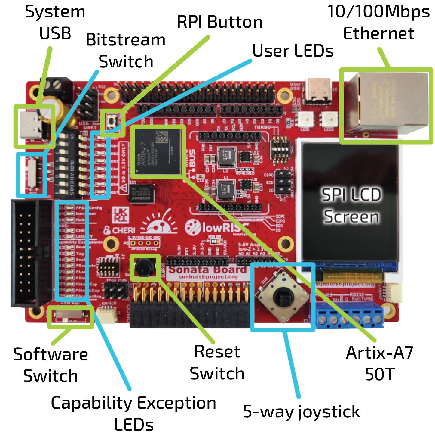
Configuration
The 'usable' requirement makes it worth thinking well about configuration. We want to provide multiple bitstreams and software images that can be switched between on the board without having to reprogram it. This is why we have a switch for bitstream and a switch for software images.
For example, we could have a CHERI and non-CHERI bitstream both available on the board. For software, we can switch between demo applications, for example CHERI compartmentalization versus CHERI exceptions. Introducing these physical switches also fulfills the 'interactive' requirement.
To make multiple bitstreams available, we introduce a USB connector that looks like mass storage to a user, where multiple bitstreams can be stored and changed without hassle. There is an RP2040 on the board to manage these configurations.
Also part of this 'usable' requirement is to have enough memory to store the bitstreams and software. We introduce two separate flash chips for these purposes and a HyperRAM chip.
Peripherals
The 'connectable' requirement means that we need to introduce common peripherals on the board. After consultation with the community, we settled on the following list:
- Ethernet
- RS-232
- RS-485
- MicroSD
- ADC
Ethernet
The Ethernet chip that is available on the PCB is KSZ8851SNLI-TR. Section 3.4 describes how to read and write registers over the SPI and Chapter 4 lists all the registers and their functionality. This datasheet is mainly useful for those needing to change the driver, so users should be able to use the driver directly, like the one provided by CHERIoT RTOS.
Headers
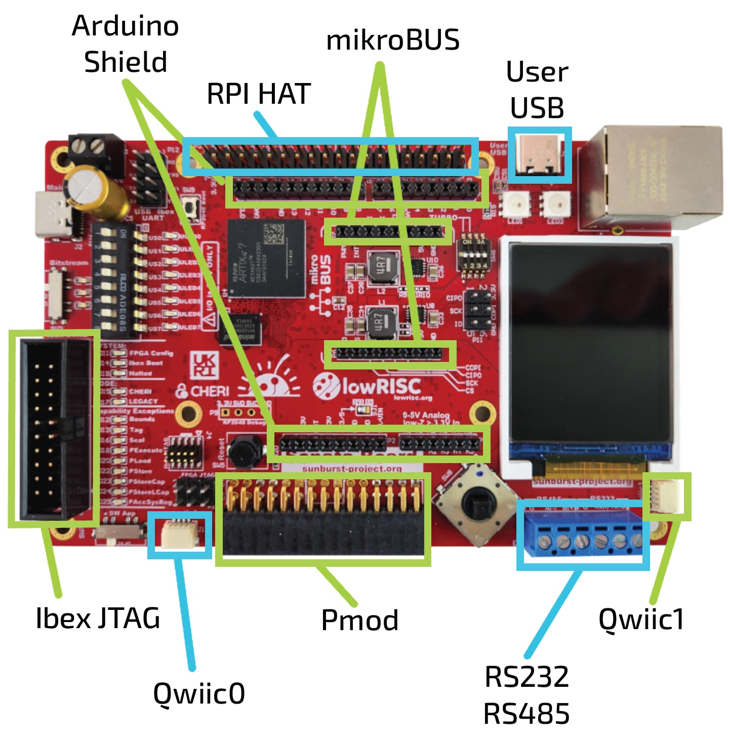
For both the 'connectable' and 'extendable' requirements, we provide a number of headers so that custom functionality can be added:
- Raspberry Pi header
- Arduino shield (only 3.3V versions supported)
- microBUS Click
- Sparkfun QWIIC
- PMOD
- 30-pin R/A header
Although, the FPGA pins can be used independently, due to the physical layout of the headers on the FPGA board, it is not possible to plug in Raspberry Pi, Arduino shield and microBUS click headers simultaneously. You can still use them simultaneously with modified wiring.
The 2 PMODs and the R/A header cannot be used at the same time since they use the same pins. We don't expect this to be a problem as most applications should only need to use one expansion board.
Debug
For ease of use, we have one USB connector that can power the board as well as debug using JTAG and two virtual UARTs. This means that users only have to connect one cable. Besides the JTAG over USB, we provide external JTAG and UART headers to enable users to use different setups if they need to.
User interface
The user interface is where we address the 'CHERI-visible' and 'interactive' requirements. In terms of user input, we have:
- DIP switches
- Button
- Joystick
In terms of output, we have:
- LEDs
- LCD screen
- CHERI-specific capability exception LEDs
Affordable
In order to meet the 'affordable' requirement, we choose a low-end FPGA to reduce the costs. We choose a Xilinx Artix 7 FPGA because it has a typical amount of memory for embedded use-cases while being able to clock the design higher than similarly priced alternatives and being supported by many tools.
Technical details
If you want to know more details on what the actual design looks like, please have a look at NewAE's repository of the Sonata PCB.
This includes the entire design sources, available currently in Altium, with a KiCad version being released shortly.
Schematic Link
You can find a direct link to the schematics for your reading pleasure.
Default DIP switch settings
We recommend the following default state for the DIP switches:
- On the front:
- SW3 "Bitstream": 2
- SW7 "SW App": 1
- SW4 "US[0-7]": all set to off
- SW6 : all set to off
- On the back:
- SW1 : all set to on
- SW2 : 1-6 set to on and 7-8 set to off
RP2040 firmware
You can build new RP2040 firmware (or find release UF2 files) from the Sonata RP2040 repository.
With that UF2 file you can now update your firmware by holding down SW9, labelled "RP2040 Boot".
While holding this button plug your Sonata board in using the main USB.
A drive called RPI-RP2 should now appear which you can drag the UF2 file onto.